

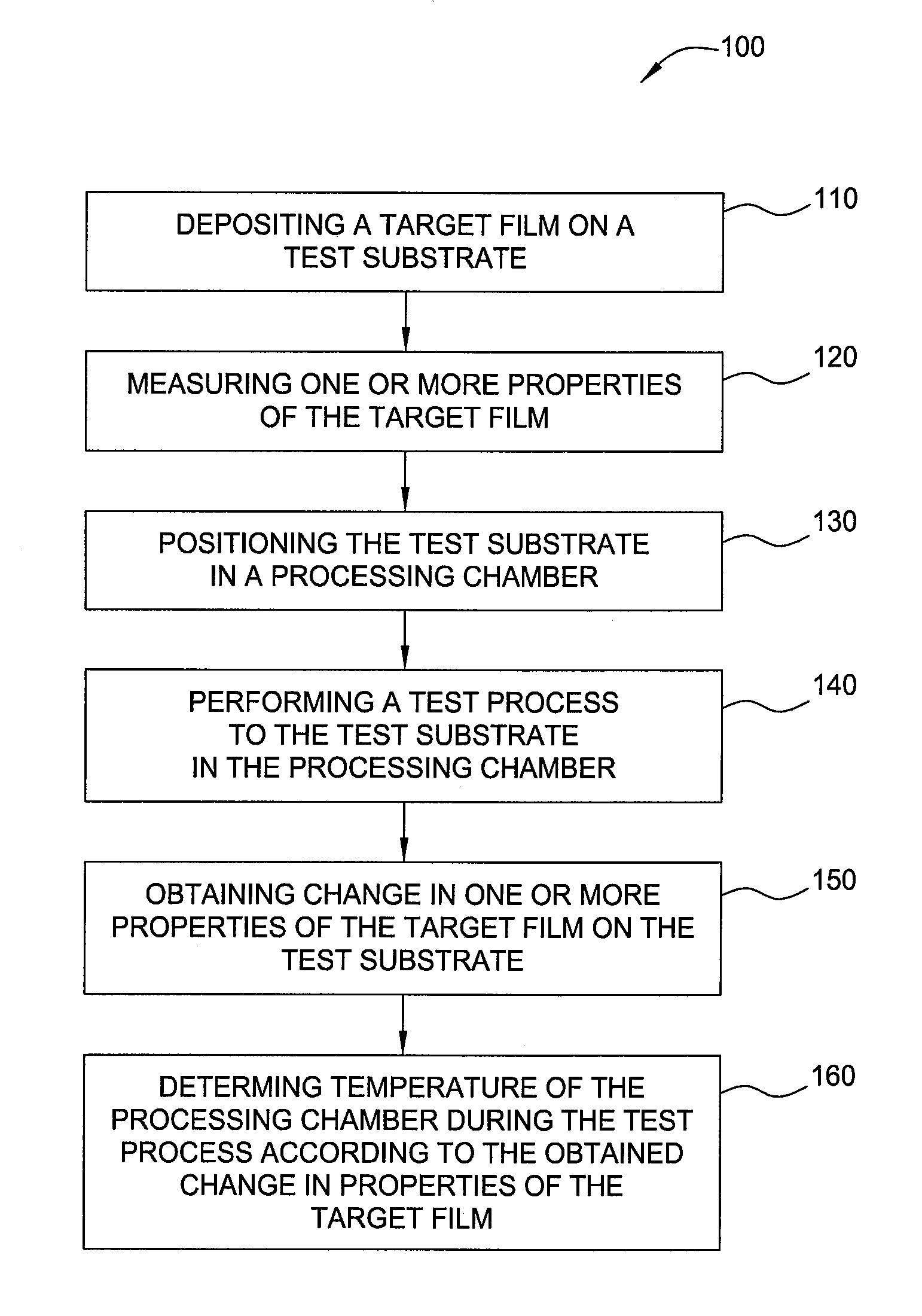
Method for monitoring and calibrating temperature in semiconductor processing chambers
a technology for monitoring and calibrating temperature in semiconductor processing chambers, applied in heat measurement, semiconductor/solid-state device testing/measurement, instruments, etc., can solve the problems of inability to effectively and non-destructively measure temperature in semiconductor processing state of the art, limited optical pyrometry to high temperatures,
- Summary
- Abstract
- Description
- Claims
- Application Information
AI Technical Summary
Benefits of technology
Problems solved by technology
Method used
Image

Examples
example
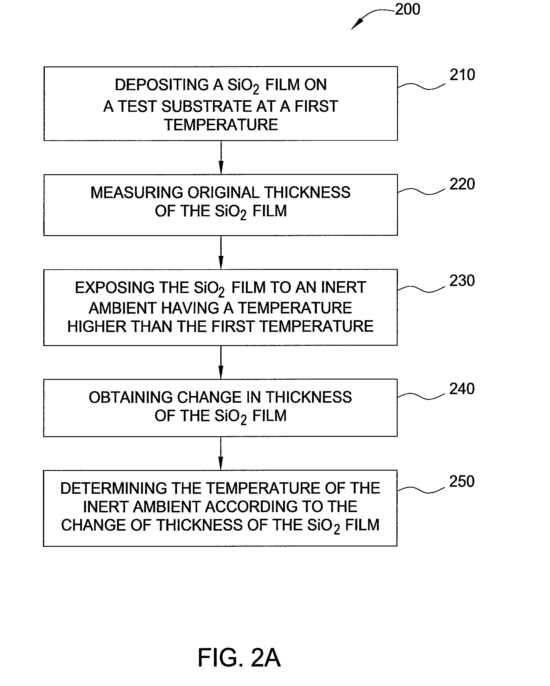
Atomic Layer Deposition of SiO2
[0045]
Chamber Pressure: 4 Torr (Pressure can be varied between 1-10 Torr)
HCDS Flow Rate: 500 sccm with Carrier Gas at 19° C.
Pyridine dosage: 500 sccm with Carrier Gas at 21° C. during HCDS flow
Water Vapor Flow Rate: 500 sccm with Carrier Gas at 30° C.
Pyridine dosage: 1000 sccm with Carrier Gas at 21° C. during Water Vapor flow
Deposition Temperature: 75° C.
Silicon Dioxide Film Thickness: about 400 Angstrom to 500 Angstrom.
[0046]Referring back to FIG. 2A, original thickness of the silicon dioxide film on the test substrate is measured, as shown in block 220. The test substrate may be stored in a low temperature environment prior to being used to measure a chamber temperature. In one embodiment, standard test substrates, test substrates with substantially the same properties, may be manufactured to eliminate measurement of the original thickness, providing accuracy and convenience to temperature measurement in accordance with the present invention.
[0047]I...
PUM
| Property | Measurement | Unit |
|---|---|---|
| temperature | aaaaa | aaaaa |
| melting temperature | aaaaa | aaaaa |
| thickness | aaaaa | aaaaa |
Abstract
Description
Claims
Application Information