Synchronous semiconductor memory device

a semiconductor and memory device technology, applied in the direction of information storage, static storage, digital storage, etc., can solve the problems of increasing the total consumption current, increasing the speed of the external clock, and increasing the required latency, so as to reduce the consumption current, increase the margin of operation timing, and control easily and immediately

Active Publication Date: 2009-08-25
NVIDIA CORP
View PDF10 Cites 21 Cited by
  • Summary
  • Abstract
  • Description
  • Claims
  • Application Information

AI Technical Summary

Benefits of technology

[0012]It is an object of the present invention to provide a synchronous semiconductor memory device having a configuration in which a rapid increase in consumption current is suppressed when using the high-speed external clock, sufficient margin for the operation timings in using the external clock is secured without being restricted by circuit operation, and various latencies which can be selectively set are reliably counted.
[0014]According to the aspect of the synchronous semiconductor memory device of the present invention, when counting various latencies corresponding to the external command, internal clocks into which the external clock is divided by two can be used, so that operation frequency becomes half of that of the high-speed external clock. Thus, effects of a decrease in consumption current and an increase in margin of the operation timing can be obtained. And when set latency is changed in detail, since a single counter circuit can count only even number latencies, two counter circuits provided in parallel enables a configuration for counting odd number latencies. In this case, a configuration is employed in which by using the normal phase clock and the reverse phase clock which are the internal clocks having a phase difference of 180 degree therebetween, the first counter circuit operates using the normal phase clock while the second counter circuit operates using the reverse phase clock, and a signal path is appropriately switched in response to the number of the clock cycles to be counted. Thereby, various latencies can be counted within a relatively wide range, regardless of whether the number is even or odd. Accordingly, a synchronous type semiconductor memory device which can count desired latencies adapting to command types or operation conditions with low consumption current can be realized.
[0022]As described above, according to the present invention, when using the internal clocks into which the external clock is divided to count the set latency, the latency counter including the first counter circuit and the second counter circuit is provided so as to form a signal path which is shifted therebetween, and thereby various latencies can be selectively counted regardless of whether the number is even or odd. And when using the high-speed external clock, the latency counter operates with the internal clocks having a half frequency, and thus a decrease in consumption current and an increase in margin of the operation timing can be realized. Further, when the set latency is changed, it is possible to control easily and immediately, and by providing many latency counters individually corresponding to external command types and operation conditions, it is possible to facilitate adjustment of operation timings in the entire semiconductor memory device.

Problems solved by technology

Further, with progress of the DDR-SDRAM generation, speed of the external clock increases and the required latency tends to gradually increase.
That is, since the internal clock having the same frequency as the external clock is applied to each stage of the nine-stage shift register, sequential shift operation of each stage performed at every period tCK of the external clock causes a problem of an increase in the entire consumption current.
In this case, it is a problem that as the speed of the external clock increases, the consumption current rapidly increases.
And since the minimum period tCKmin of the external clock is restricted by circuit operation such as transfer speed of the shift register, sufficient operation margin can not be secured, which may also cause a problem of high speed.

Method used


Image

  • Synchronous semiconductor memory device
  • Synchronous semiconductor memory device
  • Synchronous semiconductor memory device

Examples


Embodiment Construction

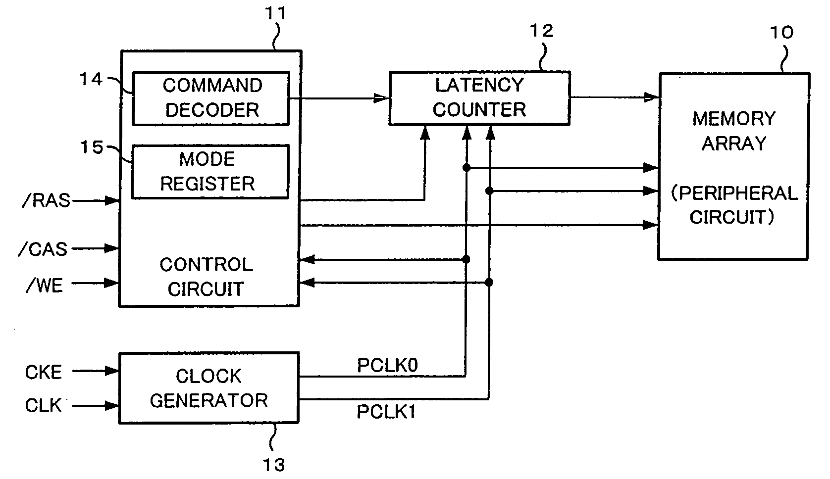
[0036]Embodiments of the present invention will be described hereinafter with reference to accompanying drawings. In this embodiment, a synchronous semiconductor memory device to which the present invention applied is, for example, a DDR-SDRAM having a latency counter for counting latencies set for various commands.

[0037]FIG. 1 is a block diagram showing a principal configuration of a synchronous semiconductor memory device of this embodiment. The synchronous semiconductor memory device as shown in FIG. 1 includes a memory array 10, a control circuit 11, a latency counter 12, and a clock generator 13. Actually the synchronous semiconductor memory device includes many other components, but only components related to the function based on the present invention are shown in FIG. 1.

[0038]In the above-mentioned configuration, the memory array 10 includes a plurality of memory cells formed at intersections of a plurality of word lines and a plurality of bit lines arranged in a matrix, and...


PUM


Abstract

A synchronous semiconductor memory device of the present invention has a clock generator for generating a normal and a reverse phase clocks by dividing an external clock, a command decoder for decoding an external command and outputting a command signal; latency setting means capable of selectively setting an even or odd number latency within a range of a predetermined number of clock cycles of the external clock, a latency counter which includes two counter circuits for sequentially shifting the command signal captured using the normal and reverse phase clock and being capable of switching a signal path in response to the number of clock cycles, and first and second control means which controls counting of the clock cycles equivalent to the even or odd number latency by forming an appropriate signal path.

Description

RELATED APPLICATIONS[0001]This application is a Divisional of U.S. application Ser. No. 11 / 583,980, filed Oct. 20, 2006, now U.S. Pat. No. 7,345,950 claiming priority of Japanese Application No. 2005-306418, filed Oct. 20, 2005, the entire contents of each of which are hereby incorporated by reference.BACKGROUND OF THE INVENTION[0002]1. Field of the Invention[0003]This invention relates to a synchronous semiconductor memory device which operates in synchronization with a clock, and particularly relates to a synchronous semiconductor memory device having a configuration for controlling operation timings corresponding to a latency after an issuance of a command for various purposes.[0004]2. Description of the Related Art[0005]Recently SDRAM (Synchronous Dynamic Random Access Memory) of DDR (Double Data Rate) type has been a mainstream as a synchronous semiconductor memory device to allow high speed operation. Since this DDR-SDRAM (referred to as DDR-SDRAM hereinafter) employs a high s...

Claims


Application Information

Patent Timeline
Patent Type & Authority Patents(United States)
IPC IPC(8): G11C8/00
CPCG11C7/22G11C11/4076G11C7/222
Inventor FUJISAWA, HIROKIKUBOUCHI, SHUICHIKUROKI, KOJI
Owner NVIDIA CORP
Why Eureka
Try Eureka