Supercharge Your Innovation With Domain-Expert AI Agents!

Liquid crystal display device and fabricating method thereof

a liquid crystal display and substrate technology, applied in non-linear optics, instruments, optics, etc., can solve the problems of high power consumption of backlight units, complicated manufacturing process, and increase of liquid crystal display panel manufacturing costs, so as to simplify the method of fabricating the same and increase the aperture ratio

Inactive Publication Date: 2009-09-01
LG DISPLAY CO LTD
View PDF24 Cites 22 Cited by
  • Summary
  • Abstract
  • Description
  • Claims
  • Application Information

AI Technical Summary

Benefits of technology

The present invention provides a liquid crystal display device with increased aperture ratio in the transmissive area and a simplified method of fabrication. The device includes a thin film transistor substrate with a double layer structure including a first transparent conductive layer and a second opaque conductive layer on the first substrate. A first insulation film is on the gate line and a second insulation film is on the data line. A pixel electrode has the first conductive layer and the second conductive layer along the boundary of the first conductive layer. A storage upper electrode is overlapping the first insulation film and the second insulation film to form a storage capacitor. A transmission hole exposing a side surface of the storage upper electrode is formed through the first insulation film and the second insulation film. A reflective electrode connecting the second conductive layer of the pixel electrode with the drain electrode and the storage upper electrode through the transmission hole is formed. The method of fabrication includes forming a gate pattern with a double layer structure, forming a first insulation film, forming a semiconductor pattern and a source / drain pattern, forming a second insulation film, forming a transmission hole, and forming a reflective electrode. The technical effects of the invention include increased aperture ratio and simplified fabrication process.

Problems solved by technology

There is a problem that the power consumption of a backlight unit is high in the transmissive type and the reflective type depends on the external light so as not to be able to display the picture in a dark environment
In such a transflective liquid crystal display panel, the thin film transistor substrate includes the semiconductor process and requires a plurality of mask processes, thus its manufacturing process is complicated so that it becomes a material cause for the increase of the liquid crystal display panel manufacturing cost.
Accordingly, the related art transflective thin film transistor substrate is formed using six 6 different mask processes, thus there is a disadvantage that its manufacturing process is complicated.
Because of this, there is a disadvantage that the aperture ratio of the transmissive area is reduced.

Method used


Image

  • Liquid crystal display device and fabricating method thereof
  • Liquid crystal display device and fabricating method thereof
  • Liquid crystal display device and fabricating method thereof

Examples


first embodiment

[0095]In this way, the fabricating method of the transflective thin film transistor substrate according to the present invention is formed using four mask processes, compared to the six mask process of the related art. Thereby simplifying the fabrication process.

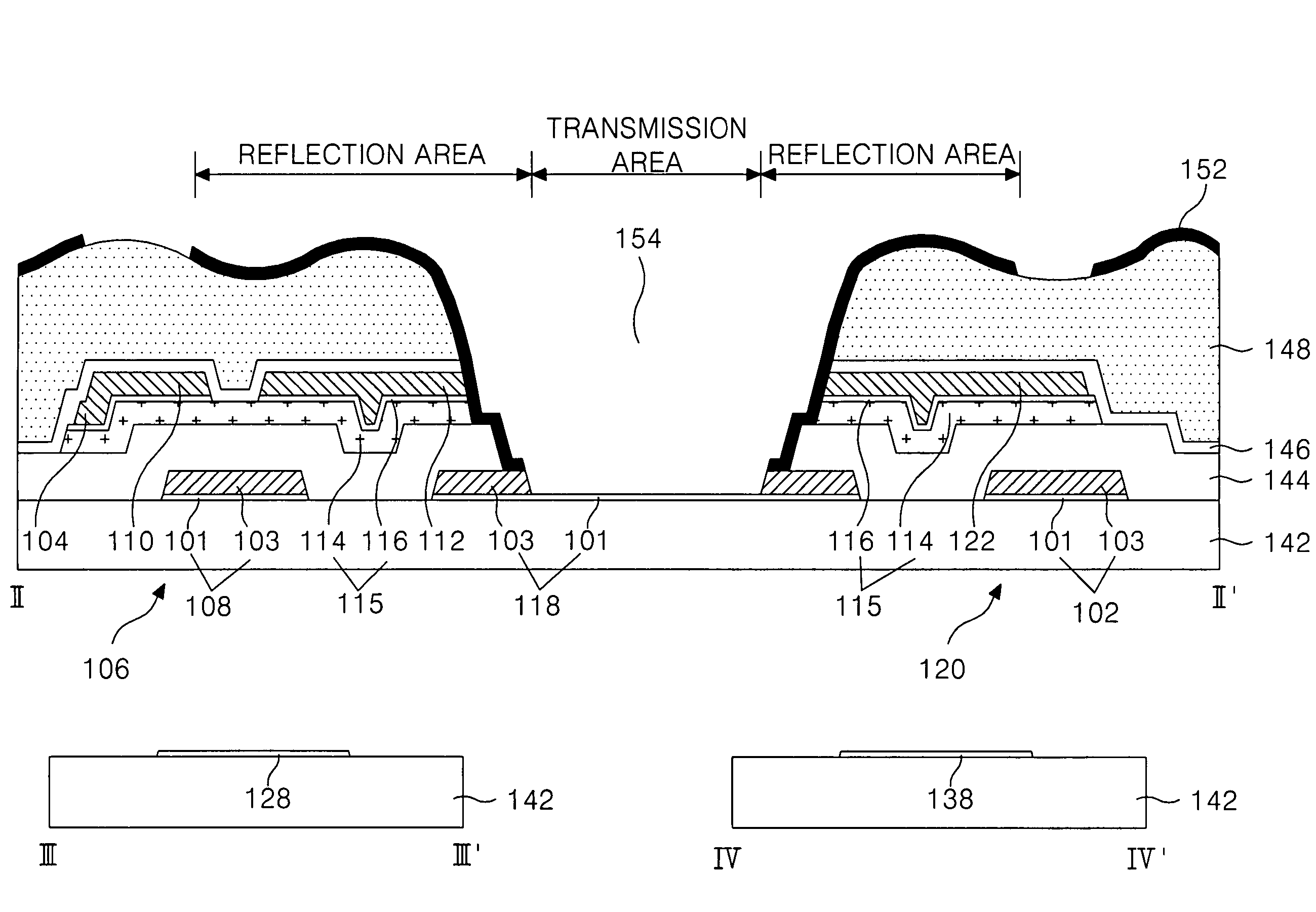
[0096]FIG. 11 is a sectional diagram illustrating a transflective thin film transistor substrate according to another embodiment of the present invention. The transflective thin film transistor substrate illustrated in FIG. 11 has the same components as the transflective thin film transistor substrate illustrated in FIG. 4 except that the gate line 102, the gate electrode 104 and the pixel electrode 118a include a third conductive layer. Accordingly, the explanation for the repeated components will be omitted.

[0097]As illustrated in FIG. 11, when the gate pattern, which includes the gate line 102, the gate electrode 104 and the pixel electrode 118, is formed on the substrate a third metal conductive layer 105, for example, A...

second embodiment

[0099]In order to prevent this, according to the invention, a third conductive layer 113 which is not easily dry etched is added to the pixel electrode to act as an etch stopper when forming the transmission hole 154, thereby preventing the second conductive layer 103 of the pixel electrode 118 from being etched. Accordingly, it is possible to prevent the first conductive layer 101 from turning black, due to dry etching of the second conductive layer 103.

[0100]The third conductive layer 113 and the second conductive layer 103 are removed during the wet etching process form the reflective electrode 152 by the fourth mask process, as described above with respect to the first embodiment.

[0101]FIG. 13 illustrates an ambient part of the transflective thin film transistor substrate according to the present invention. As

[0102]The transflective thin film transistor substrate 100 illustrated in FIG. 4 includes a contact electrode 160 connecting the data pad 138, formed in the same layer as t...

third embodiment

[0116]FIG. 20 is a plane view illustrating a transflective thin film transistor substrate according the present invention, and FIG. 21 is a sectional diagram illustrating the transflective thin film transistor substrate shown in FIG. 20, taken along the lines VII-VII′, VIII-VIII′, III-III′ and IV-IV′.

[0117]The transflective thin film transistor substrate includes in FIGS. 20 and 21 includes the same components as the transflective thin film transistor substrate shown in FIGS. 3 and 4 except that a storage line 425 in parallel to the gate line 102 is added, and a storage capacitor 420 is formed to overlap a storage lower electrode 423 which is integrated with the storage line 425 and a storage upper electrode 422 which is integrated with the drain electrode 112. Accordingly, explanation for the repeated components is to be omitted. The ambient part of the transflective thin film transistor substrate and the fabricating method thereof are as described above in FIGS. 12 to 19B.

[0118]Th...


PUM

PropertyMeasurementUnit
transparent conductiveaaaaaaaaaa
conductiveaaaaaaaaaa
transmissive areaaaaaaaaaaa

Abstract

A liquid crystal display device is provided that includes: first and second substrates; a gate line of a double layer having a first transparent conductive layer and a second opaque conductive layer on the first substrate; a first insulation film on the gate line; a data line crossing the gate line to define a pixel region, the pixel region having a transmissive area and a reflective area; a thin film transistor connected to the gate and data lines; a pixel electrode having the first conductive layer in the pixel region and a second conductive layer along the boundary of the first conductive layer; a storage upper electrode to form a storage capacitor by overlapping with the gate line the first insulation film there between; a transmission hole to expose the side of the storage upper electrode and a drain electrode of the thin film transistor by passing through the first insulation film and a second insulation film on the thin film transistor; a reflective electrode connected the second conductive layer of the pixel electrode with the drain electrode and the storage upper electrode through an edge portion of the transmission hole; and a liquid crystal layer between the first and second substrates.

Description

[0001]This application claims the benefit of Korean Patent Application No. P2004-41142, filed on Jun. 5, 2004, which is hereby incorporated by reference for all purposes as if fully set forth herein.BACKGROUND OF THE INVENTION[0002]1. Field of the Invention[0003]The present invention relates to a thin film transistor (TFT) substrate of a transflective liquid crystal display device and more particularly to simplified process for fabricating a transflective TFT transistor substrate.[0004]2. Description of the Related Art[0005]Liquid crystal display devices are generally classified into two types: the transmissive type in which pictures are displayed using light supplied from a backlight unit, and the reflective type in which pictures are displayed using light reflected from an external source, such as natural light. There is a problem that the power consumption of a backlight unit is high in the transmissive type and the reflective type depends on the external light so as not to be ab...

Claims


Application Information

Patent Timeline
Patent Type & Authority Patents(United States)
IPC IPC(8): G02F1/1335G02F1/1362G02F1/136G02F1/1368
CPCG02F1/133555G02F1/1362G02F2001/136231G02F1/136231G02F1/136
Inventor AHN, BYUNG CHUL
Owner LG DISPLAY CO LTD
Features
  • R&D
  • Intellectual Property
  • Life Sciences
  • Materials
  • Tech Scout
  • Unparalleled Data Quality
  • Higher Quality Content
  • 60% Fewer Hallucinations
Learn More