Active array substrate for a liquid crystal display

a liquid crystal display and active array technology, applied in non-linear optics, instruments, optics, etc., can solve the problems of further affecting display quality, a higher load on scan lines, etc., to enhance contrast uniformity, enhance brightness, and improve waveform passing distortion

Active Publication Date: 2009-09-15
AU OPTRONICS CORP
View PDF4 Cites 30 Cited by
  • Summary
  • Abstract
  • Description
  • Claims
  • Application Information

AI Technical Summary

Benefits of technology

[0009]The object of the present invention is to provide an active array substrate, which can improve the distortion of waveform passing through the scan line to thereby enhance the brightness, enhance contrast uniformity, and reduce the image flicker phenomenon of the liquid crystal display.

Problems solved by technology

In general, as compared with the structure of storage capacitance on a common line (hereinafter, referring to as “Cs on Common”) that is produced by overlapping a common line and a pixel electrode, the pixels formed by the structure “Cs on Gate” have the advantage of preferred aperture ratio because the storage capacitance is stacked on the scan line without additional affecting the aperture ratio, but also have the disadvantage of suffering a higher load on the scan line due to the capacitance connected in series on the scan line.
As shown in FIGS. 1A and 1B, the waveform passing through the scan line is gradually changed and distorted, which causes at least one of the non-uniform brightness, the non-uniform contrast, and frame flicker of the LCD, and further affects the display quality.

Method used


Image

  • Active array substrate for a liquid crystal display
  • Active array substrate for a liquid crystal display
  • Active array substrate for a liquid crystal display

Examples


Embodiment Construction

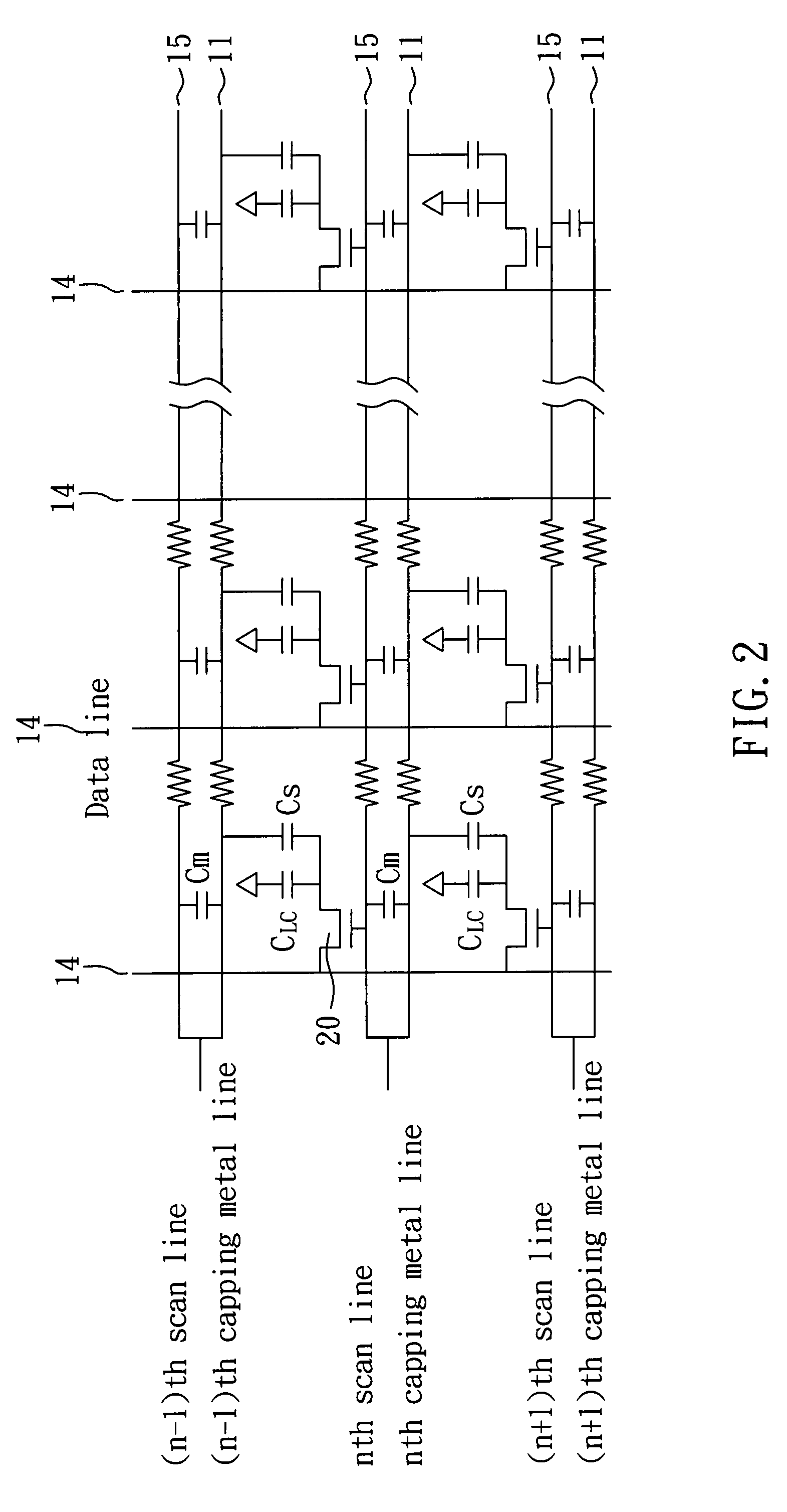
[0028]FIG. 2 shows a schematic diagram of a display circuit according to one embodiment of the present invention.

[0029]As shown in FIG. 2, the display circuit forms a minor capacitance Cm between a capping metal line and a scan line.

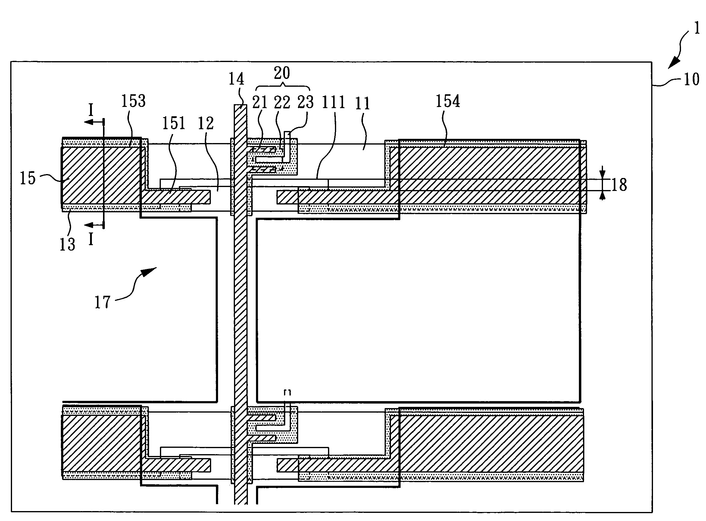
[0030]FIGS. 3A to 3D are a schematic flowchart of producing an active array substrate equivalent to the display circuit of FIG. 2 according to the embodiment of the present invention. FIG. 4 is a cross-sectional view of the substrate at the notation I-I of FIG. 3D according to the embodiment of the present invention. The following is described by referring to both of FIGS. 3A-3D and 4.

[0031]In FIG. 3D, the active array substrate 1 for an LCD includes a plurality of switches 20, a plurality of first scan lines 11, a plurality of second scan lines 15, a plurality of data lines 14, and a plurality of pixel electrodes 17. In addition, each second scan line 15 includes a plurality of auxiliary connection pads 12.

[0032]The process for the substrate 1 is starte...


PUM

PropertyMeasurementUnit
total minor capacitanceaaaaaaaaaa
total resistanceaaaaaaaaaa

Abstract

An active array substrate for an LCD is disclosed. The active array substrate uses one end of the second scan line to electrically connect to the first scan line and electrically insulates the remaining second scan line from the first scan line. Accordingly, the second scan lines can be shielded the voltage of the transmission waveform on the first scan lines, and obtain a result of reduce a distortion level of a waveform, enhance the uniformity of the brightness, enhance the contrast of the LCD, and reduce the image flicker phenomenon of the LCD.

Description

BACKGROUND OF THE INVENTION[0001]1. Field of the Invention[0002]The present invention relates to an active array substrate and, more particularly, to an active array substrate for a liquid crystal display (LCD).[0003]2. Description of Related Art[0004]In reference to LCD panel technologies, the structure of storage capacitance Cs on a scan line (hereinafter, referring to as “Cs on Gate”) is designed and produced by implementing and overlapping an insulation layer between a scan line and a pixel electrode.[0005]In general, as compared with the structure of storage capacitance on a common line (hereinafter, referring to as “Cs on Common”) that is produced by overlapping a common line and a pixel electrode, the pixels formed by the structure “Cs on Gate” have the advantage of preferred aperture ratio because the storage capacitance is stacked on the scan line without additional affecting the aperture ratio, but also have the disadvantage of suffering a higher load on the scan line due ...

Claims


Application Information

Patent Timeline
Patent Type & Authority Patents(United States)
IPC IPC(8): G02F1/136G02F1/1343
CPCG02F1/136286G02F2001/13629G02F1/13629
Inventor LAI, CHI-KUANG
Owner AU OPTRONICS CORP
Why Eureka
Try Eureka