Wired circuit board assembly sheet

a wired circuit board and assembly sheet technology, applied in the direction of printed circuit repair/correction, circuit inspection/indentification, printed circuit aspects, etc., can solve the problem of difficult identification of the wired circuit board to which each alignment mark corresponds, and achieve easy and reliable removal of the removal portion, excellent electric characteristics, and reduced abrasion of the stamping die

Inactive Publication Date: 2009-09-22
NITTO DENKO CORP
View PDF30 Cites 8 Cited by
  • Summary
  • Abstract
  • Description
  • Claims
  • Application Information

AI Technical Summary

Benefits of technology

[0011]To improve the productivity of the wired circuit board and reduce the production cost thereof, it is necessary to arrange the wired circuit boards at a high density in a single wired circuit board assembly sheet. However, in the wired circuit board assembly sheet in which the wired circuit boards are arranged at a high density, the region in which the defect-distinguishing mark can be formed is small so that the plurality of wired circuit boards are in close proximity to one of the defect-distinguishing marks. In such a case of the circular alignment marks disclosed in Japanese Unexamined Patent Publication No. 2001-127399, it is difficult to identify the wired circuit board to which each alignment mark corresponds.
[0024]When the supporting sheet has the openings formed in the portions where the distinguishing marks are formed and each of the distinguishing marks comprises the removal portion for indicating whether the corresponding wired circuit board is defective or non-defective and the joint portion made of a resin for jointing the removal portion to the supporting sheet, the removal portion can be easily removed from the supporting sheet by cutting the joint portion to show whether the wired circuit board is defective or non-defective. Because the joint portion is made of a resin, there is no production of metal powder or the like even when the joint portion is cut so that the wired circuit board is allowed to retain its excellent electric characteristics. Even when punching is performed with a stamping die, the abrasion of the stamping die can be reduced. As a result, it is possible to easily and reliably remove the removal portion to provide the wired circuit board with high connection reliability.

Problems solved by technology

In such a case of the circular alignment marks disclosed in Japanese Unexamined Patent Publication No. 2001-127399, it is difficult to identify the wired circuit board to which each alignment mark corresponds.

Method used


Image

  • Wired circuit board assembly sheet
  • Wired circuit board assembly sheet
  • Wired circuit board assembly sheet

Examples


Embodiment Construction

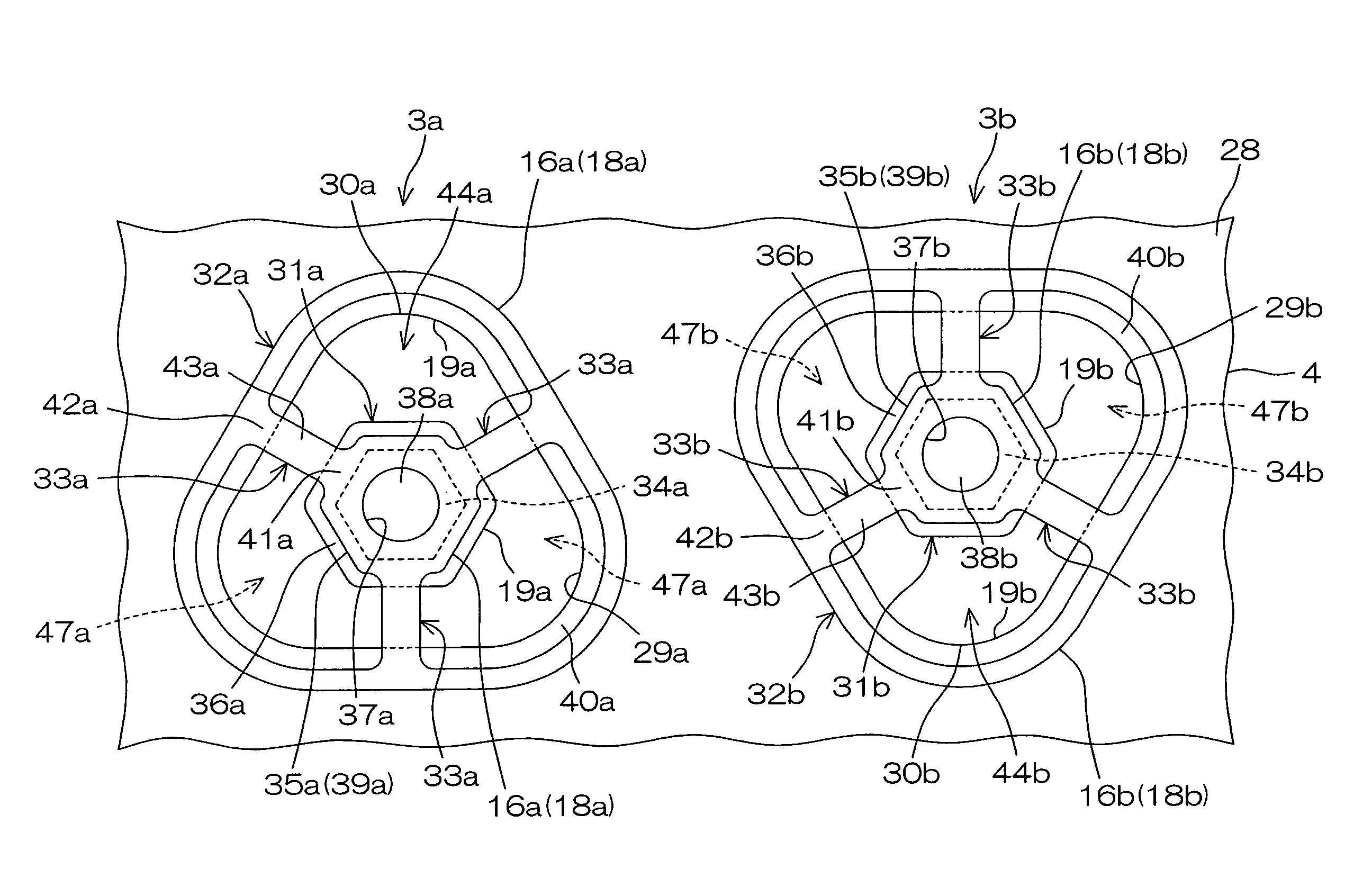
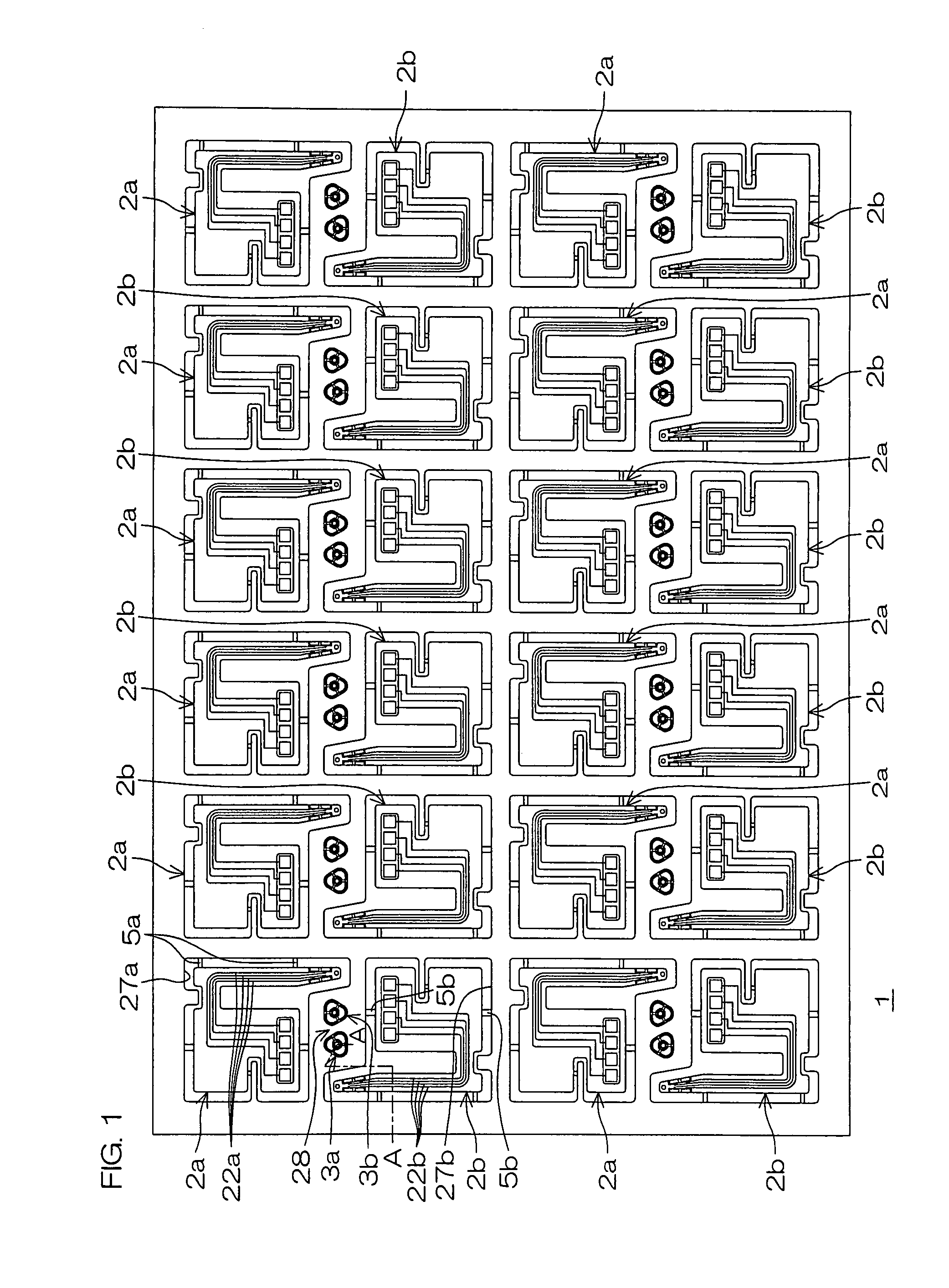
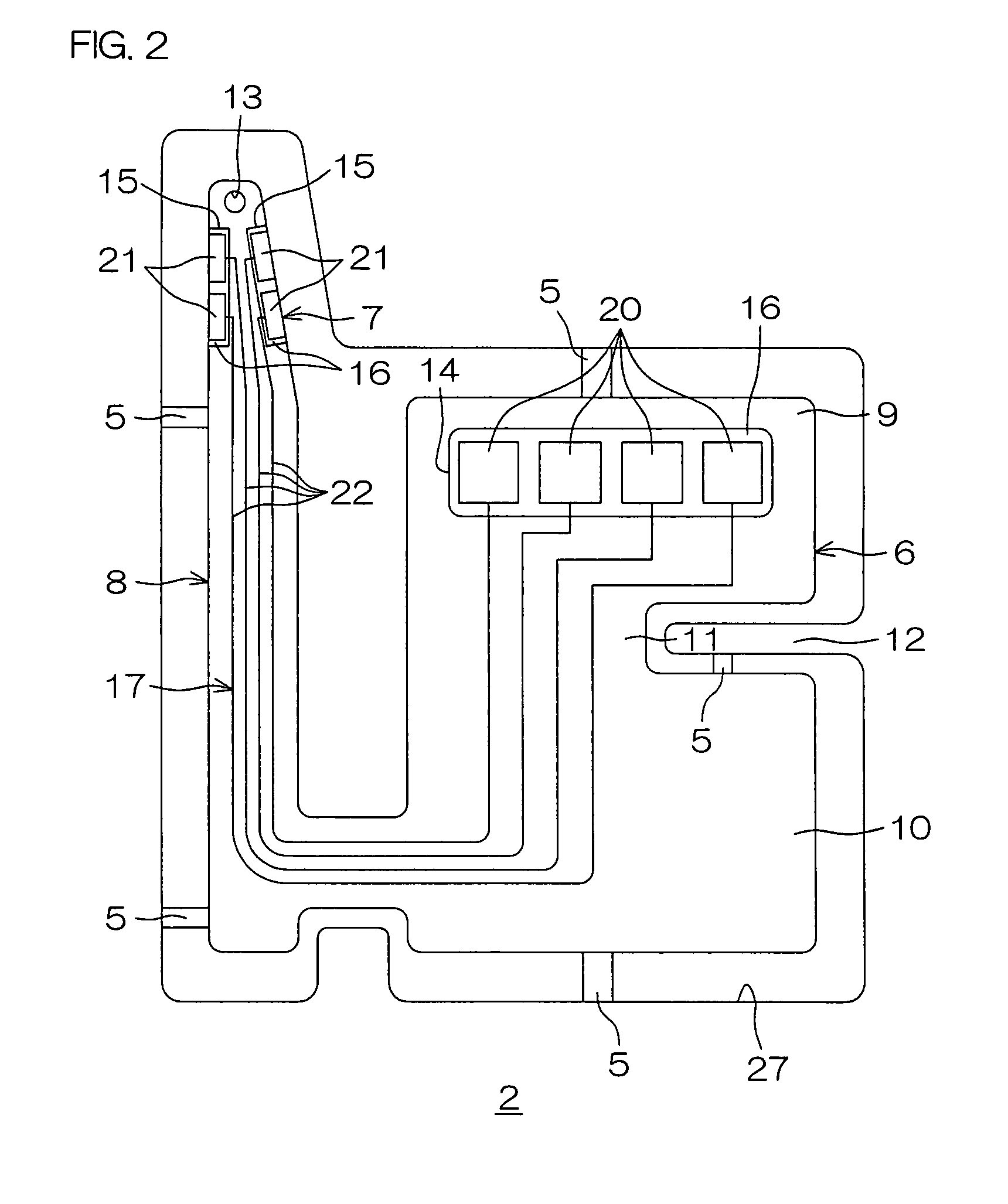
[0048]FIG. 1 is a plan view showing a wired circuit board assembly sheet according to an embodiment of the present invention. FIG. 2 is a plan view of one of the wired circuit boards shown in FIG. 1. FIG. 3 is a bottom view showing a placement of a metal supporting layer in the wire circuit board shown in FIG. 2. FIG. 4 is a cross-sectional view taken along the line A-A of the wire circuit board assembly sheet shown in FIG. 1. FIG. 5 is an enlarged plan view of a distinguishing mark formation region formed in the wired circuit board assembly sheet shown in FIG. 1. In FIG. 1, an insulating base layer 16 and an insulating cover layer 18, described later are omitted.

[0049]In FIG. 1, a wired circuit board assembly sheet 1 comprises a plurality of wired circuit boards 2, distinguishing marks 3, and a supporting sheet 4 for supporting the plurality of wired circuit boards 2 and the distinguishing marks 3.

[0050]In the supporting sheet 4, the respective wired circuit boards 2 are provided i...


PUM

PropertyMeasurementUnit
thicknessaaaaaaaaaa
thicknessaaaaaaaaaa
widthaaaaaaaaaa

Abstract

A wired circuit board assembly sheet having a plurality of wired circuit boards, distinguishing marks for distinguishing defectiveness of the wired circuit boards, and a supporting sheet for supporting the plurality of wired circuit boards and the distinguishing marks. Each of the distinguishing marks has an indication portion for indicating a specified wired circuit board.

Description

CROSS-REFERENCE TO RELATED APPLICATION[0001]The present application claims priority from Japanese Patent Application No. 2006-111163 filed on Apr. 13, 2006, the content of which is hereby incorporated by reference into this application.BACKGROUND OF THE INVENTION[0002]1. Field of the Invention[0003]The present invention relates to a wired circuit board assembly sheet in which a plurality of wired circuit boards are formed.[0004]2. Description of Related Art[0005]A wired circuit board typically comprises an insulating base layer, a conductive pattern formed on the insulating base layer, and an insulating cover layer formed on the insulating base layer to cover the conductive pattern. Such a wired circuit board is produced as a wired circuit board assembly sheet in which, e.g., a plurality of wired circuit boards are formed on a single metal supporting board.[0006]More specifically, in the production of the wired circuit board assembly sheet, the insulating base layer, the conductive ...

Claims


Application Information

Patent Timeline
Patent Type & Authority Patents(United States)
IPC IPC(8): H05K1/00
CPCH05K1/0269Y10T29/49131H05K3/0052H05K3/225H05K2201/0909H05K2201/09127H05K2201/0969H05K2201/09781Y10T29/53026Y10T29/49133Y10T29/53035Y10T29/53039Y10T29/53043Y10T29/4913Y10T29/53022Y10T29/5303H05K1/056
Inventor NAITO, TOSHIKIOHSAWA, TETSUYAKATAOKA, KOUJI
Owner NITTO DENKO CORP
Why Eureka
Try Eureka