

Semiconductor device
a technology of semiconductors and resistors, applied in the direction of semiconductor devices, electrical equipment, transistors, etc., can solve the problems of reducing the effective value of resistor r and being extremely difficult to cop
- Summary
- Abstract
- Description
- Claims
- Application Information
AI Technical Summary
Benefits of technology
Problems solved by technology
Method used
Image

Examples
first embodiment
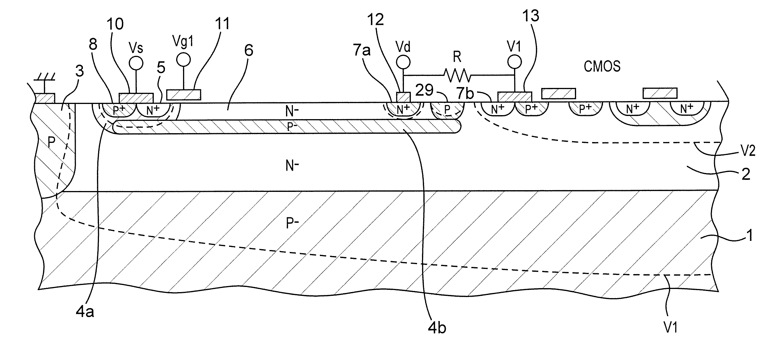
[0043]A semiconductor device of the present first embodiment is a drive circuit for gates of insulated-gate bipolar transistors (IGBTs) 61 and 62 provided on a P type substrate 1 in one of which surfaces an N− epitaxial layer 2 is formed, which drive circuit includes, as shown in FIG. 4, a high side control logic 51 and a low side control logic 52 connected to the respective gates of the IGBTs 61 and 62 and two level shift circuits each of which is constituted of an NMOSFET 31 and a resistor R.
[0044]Specifically, as shown in FIG. 3B, the high side control logic 51 and the low side control logic 52 are formed in a CMOS region of the P type substrate 1 and the two NMOSFETs 31 are arranged side by side in a condition where they are separated from each other by a P region 4, in such a configuration that the resistor R is arranged between each of the NMOSFETs 31 and the high side control logic 51 in the CMOS region.
[0045]A CMOS transistor in this CMOS region operates on a floating power ...
modified example 1
[0071]Although it has been pointed out that preferably a triple-resurf structure is applied to a portion where an NMOSFET is configured in the above description of the first embodiment, a double-resurf structure, for example, may be applied to a portion other than those where the NMOSFET is configured.
[0072]However, in a case where a triple-resurf structure is applied to a portion where an NMOSFET is configured, it is preferable that the triple-resurf structure is also applied also to a portion other than those where the NMOSFET is configured.
[0073]Specifically, a laminated structure including an N type layer, a P type layer, and an N type layer laminated in this order from the substrate 1 is formed adjacent to a portion other than those where an NMOSFET is configured, and impurity concentrations of these N type layer, P type layer, and N type layer of this laminated structure are set in such a manner that an electric field on the surface is uniform. An example where a triple-resurf...
modified example 2
[0075]In the first embodiment, the P− region 4b or the P− region 4c has been provided on both sides of a portion where an NMOSFET is formed. However, in the present invention the N− epitaxial layer 2 may be exposed in place of the P− region 4b or the P− region 4c provided on both sides of a portion where an NMOSFET is formed.
[0076]In such a case, a region where the NMOSFET is formed has a triple-resurf structure and portions other than this region have an ordinary resurf structure. Accordingly, it is necessary to form the N− layer 2 so as to satisfy ordinary resurf conditions, and to form the P− layer 4b and the N− layer 6 as shallow as possible so as not to greatly deviate from triple-resurf conditions in the NMOSFET region.
[0077]However, a fatal problem does not occur, since an upper limit is set to an accumulation concentration in the resurf conditions, and the present structure encounters a deviation only in a direction of decreasing accumulation concentrations. Further, a major...
PUM
 Abstract
Description
Claims
Application Information