Active device, driving circuit structure, and display panel

a technology of active devices and circuit structures, applied in the field of electronic devices, can solve the problems of affecting the performance of tfts and the enhancement of tfts, and achieve the effects of improving the performance of active devices, facilitating quality, and efficiently utilizing layout spa

Active Publication Date: 2014-04-15
AU OPTRONICS CORP
View PDF7 Cites 2 Cited by
  • Summary
  • Abstract
  • Description
  • Claims
  • Application Information

AI Technical Summary

Benefits of technology

[0032]In view of the above, in the invention, an etching stop layer formed on a semiconductor layer substantially covers most area of the substrate such that a source and a drain of an active device are connected with the semiconductor layer via contact openings in the etching stop layer. Accordingly, the source and the drain substantially are disposed on the etching stop layer and thereby unnecessary parasitic currents produced between the source and the drain can be reduced so as to enhance the performance of the active device. In addition, an embodiment according to the invention includes the design of capacitor electrode patterns formed in part of the gaps of the structure of the gate. The capacitor electrode patterns can be overlapped with the source to form a first capacitor structure, which is conducive to efficiently utilize the layout space. The driving circuit structure and the display panel in the embodiments of the invention can also have favorable quality because of having such an active device.

Problems solved by technology

However, parasitic currents may occur between sources and drains such that performance of TFT is impacted.
As a result, even if channels of the TFT are fabricated with the oxide semiconductor materials, performance of the TFTs remains little enhancement.

Method used


Image

  • Active device, driving circuit structure, and display panel
  • Active device, driving circuit structure, and display panel
  • Active device, driving circuit structure, and display panel

Examples


Embodiment Construction

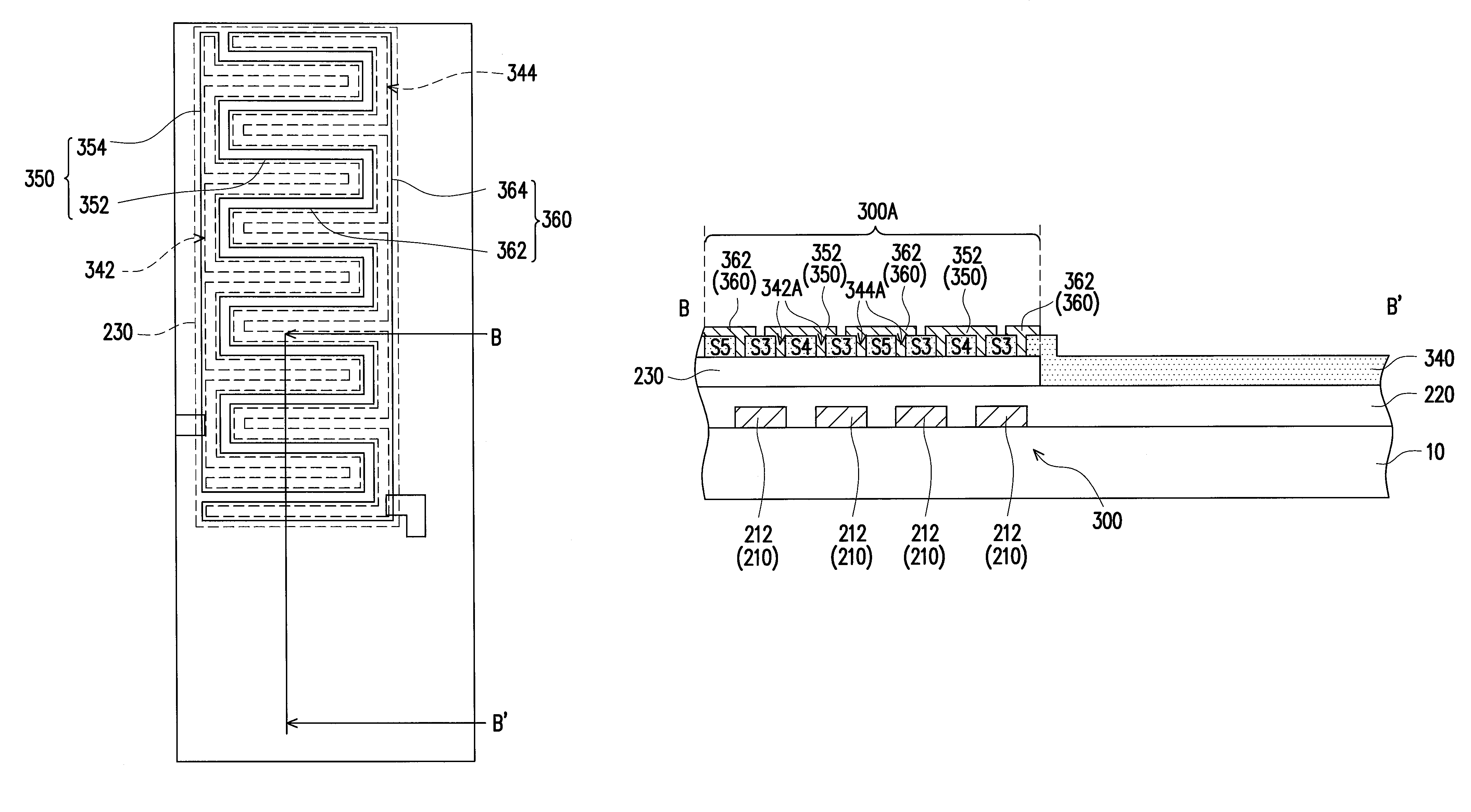
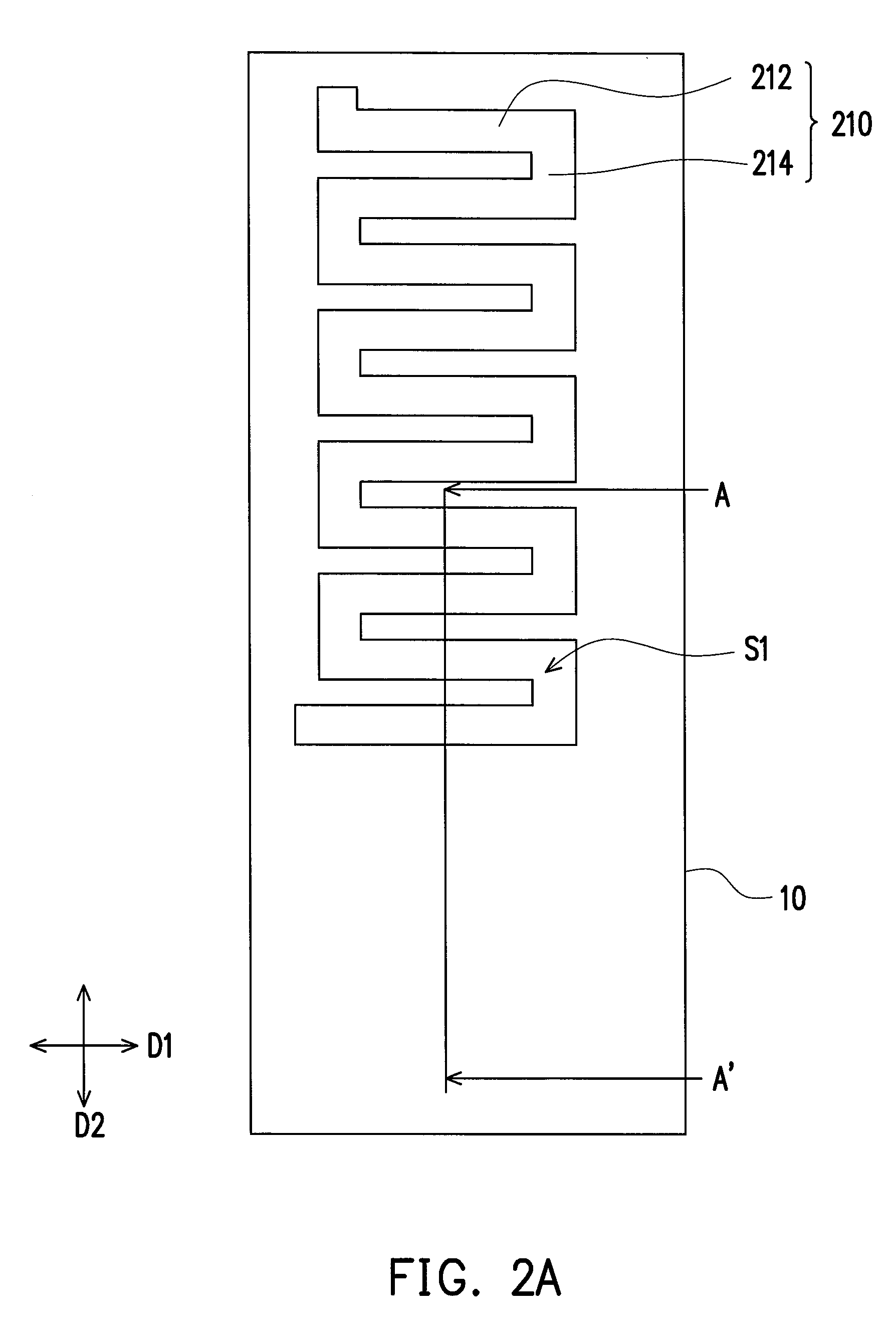
[0044]A thin film transistor (TFT) can control the transmissions of electronic signals and usually plays a role of switch in the electronic device to carry out needed functions. Since TFT can be applied in broad fields, embodiments below depicting an active device disposed in a display panel are taking as examples to illustrate an active device design provided in the invention. The active device according to the invention can be disposed in at least one of the display region and the peripheral region of a display panel. In specific, the active device of the invention can be disposed in the peripheral region, the display region or both. In an embodiment, the active device as depicted in the following embodiments can be preferably disposed in the peripheral region. Furthermore, the active device illustrated in the embodiments below can also be applied to other electronic devices, and the invention is not limited thereto.

[0045]FIG. 1 is a schematic view illustrating an electronic devic...


PUM


Abstract

An active device, a driving circuit structure, and a display panel are provided. The active device includes a gate, a gate insulation layer covering the gate, a semiconductor layer disposed above the gate, an etching stop layer disposed on the gate insulation layer and the semiconductor layer, a source, and a drain. The gate forms a meandering pattern on a substrate. The semiconductor layer has an area substantially defining a device region where the active device is. The etching stop layer has a first contact opening and a second contact opening. The first contact opening and the second contact opening separated from each other and both exposing the semiconductor layer. The source and the drain separated from each other are disposed on the etching stop layer and in contact with the semiconductor layer through the first contact opening and the second contact opening, respectively.

Description

CROSS-REFERENCE TO RELATED APPLICATION[0001]This application claims the priority benefit of Taiwan application serial no. 101120694, filed on Jun. 8, 2012 and Taiwan application serial no. 101130468, filed on Aug. 22, 2012. The entirety of each of the above-mentioned patent applications is hereby incorporated by reference herein and made a part of this specification.BACKGROUND OF THE INVENTION[0002]1. Field of the Disclosure[0003]The document relates to an electronic device; and more particularly, to an active device, a driving circuit structure and a display panel.[0004]2. Description of Related Art[0005]According to recent researches, an oxide semiconductor thin film transistor (TFT) has relatively higher carrier mobility than that of the amorphous silicon (a-Si) TFT, and threshold voltage (Vth) uniformity of the oxide semiconductor TFT is better than that of the low temperature polycrystalline silicon (LTPS) TFT. For this reason, the oxide semiconductor TFT has potential for beco...

Claims


Application Information

Patent Timeline
Patent Type & Authority Patents(United States)
IPC IPC(8): H01L29/04
CPCH01L29/786H01L29/42384H01L29/41733H01L29/78696H01L29/7869H01L29/423H01L27/1255H01L29/417
Inventor YANG, CHAO-YUCHIU, HAO-LINTSAO, SHU-WEIHUANG, SHIH-CHEYEH, PO-LIANGLIN, CHUN-NANTSENG, SHINE-KAI
Owner AU OPTRONICS CORP
Why Eureka
Try Eureka