Semiconductor integrated circuit

a technology of integrated circuits and semiconductors, applied in the direction of semiconductor devices, electrical devices, and arrangements responsive to excess voltage, can solve the problems of excessive capacitance, deterioration of lsi reliability, and increase of power consumption of electronic devices equipped with lsi, so as to prevent the increase of capacitance

Active Publication Date: 2011-08-23
PANASONIC SEMICON SOLUTIONS CO LTD
View PDF18 Cites 0 Cited by
  • Summary
  • Abstract
  • Description
  • Claims
  • Application Information

AI Technical Summary

Benefits of technology

[0011]The present invention was conceived in view of the above circumstances and provides a semiconductor integrated circuit in which generation of an unnecessary current while the power to the LSI is off is prevented and increase in capacitance is prevented.

Problems solved by technology

This can lead to an increase in power consumption of an electronic device equipped with an LSI as well as deterioration in reliability of the LSI itself.
However, the capacitance of the NMOS transistor is much larger than that of the diode, and hence, this structure has an excessively large capacitance as compared with the circuit shown in FIG. 4.

Method used


Image

  • Semiconductor integrated circuit
  • Semiconductor integrated circuit
  • Semiconductor integrated circuit

Examples


embodiment 1

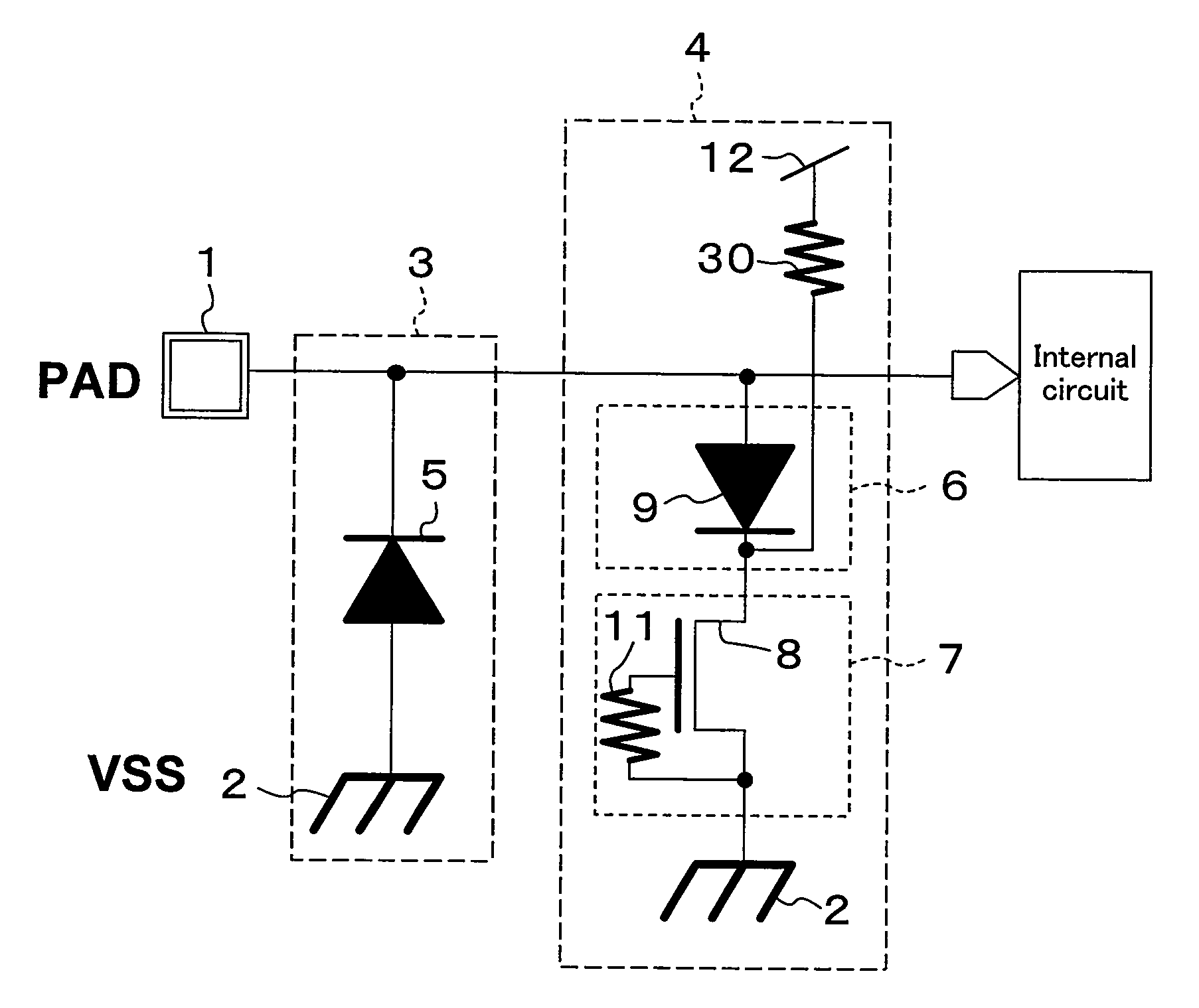
[0020]FIG. 1 shows the circuit structure of a semiconductor integrated circuit according to embodiment 1 of the present invention. In the example shown in FIG. 1, a voltage supply line is realized by a ground line.

[0021]As shown in FIG. 1, the semiconductor integrated circuit of embodiment 1 includes an external pad 1 for input or output of signals, an internal circuit connected to the external pad 1, a ground line 2, a first protection circuit 3 which is connected to a connection path extending between the external pad 1 and the internal circuit and which is provided between the external pad 1 and the ground line 2, and a second protection circuit 4 which is connected to the connection path extending between the external pad 1 and the internal circuit and which is provided between the external pad 1 and the ground line 2. It should be noted that an input circuit, output circuit, input / output circuit, or the like, may be provided between the ESD protection circuit formed by the firs...

embodiment 2

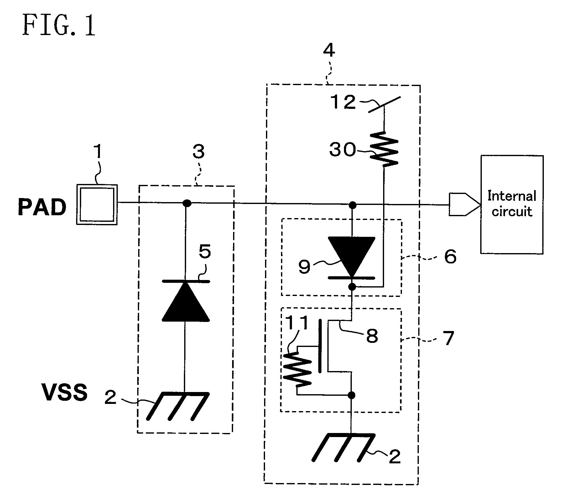
[0034]FIG. 2 shows the circuit structure of a semiconductor integrated circuit according to embodiment 2 of the present invention.

[0035]As shown in FIG. 2, the semiconductor integrated circuit of embodiment 2 includes an external pad 1, an internal circuit connected to the external pad 1, a ground line 2, a first protection circuit 3 which is connected to a connection path extending between the external pad 1 and the internal circuit and which is provided between the external pad 1 and the ground line 2, and a second protection circuit 4 which is connected to the connection path extending between the external pad 1 and the internal circuit and which is provided between the external pad 1 and the ground line 2.

[0036]The first protection circuit 3 has a first diode 5 which has the anode connected to the ground line 2 and the cathode connected to the external pad 1.

[0037]The second protection circuit 4 is formed by a first protection element 6, a second protection element 7, and a resi...

embodiment 3

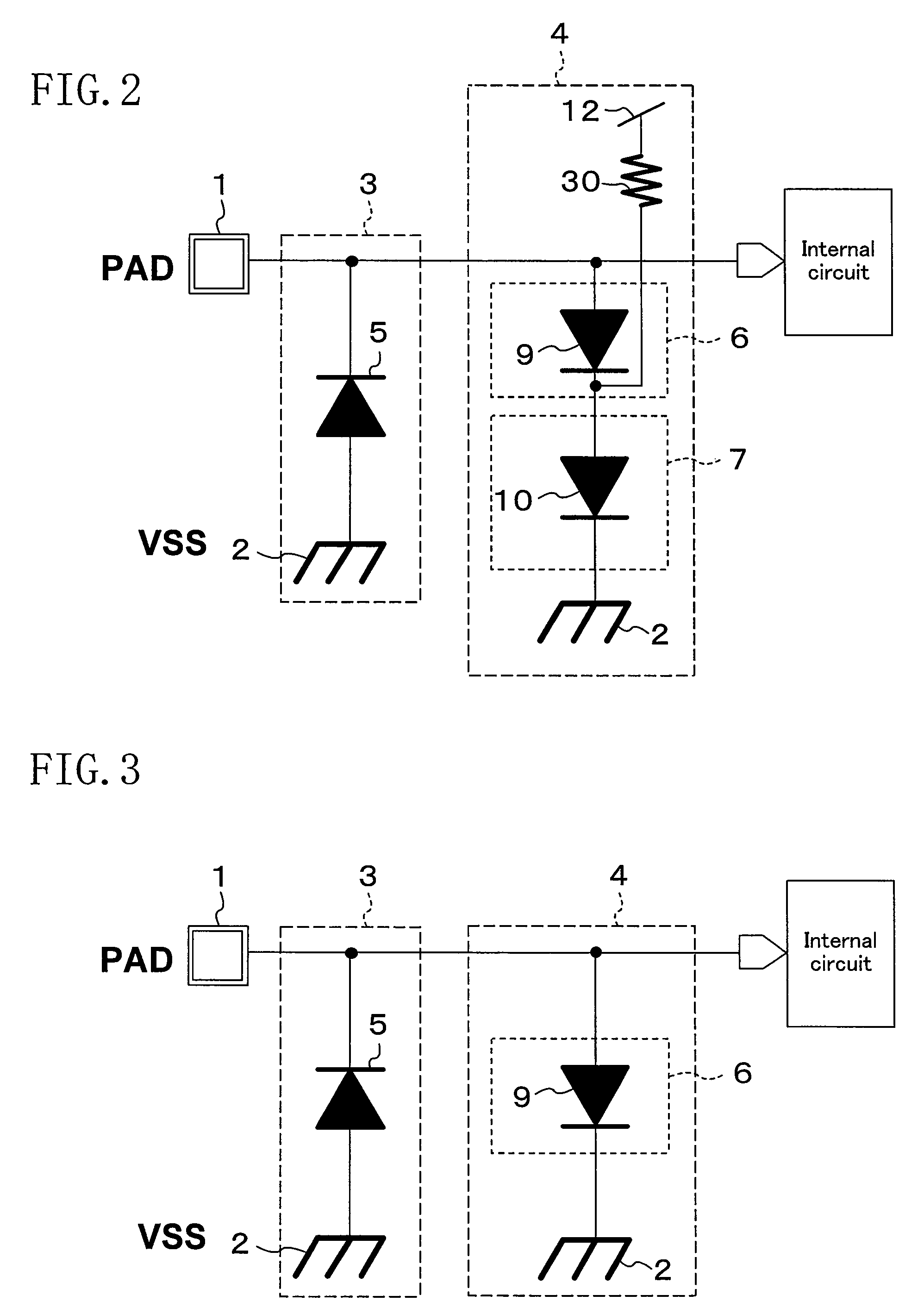
[0047]FIG. 3 shows the circuit structure of a semiconductor integrated circuit according to embodiment 3 of the present invention.

[0048]As shown in FIG. 3, the semiconductor integrated circuit of embodiment 3 includes an external pad 1, an internal circuit connected to the external pad 1, a ground line 2, a first protection circuit 3 which is connected to a connection path extending between the external pad 1 and the internal circuit and which is provided between the external pad 1 and the ground line 2, and a second protection circuit 4 which is connected to the connection path extending between the external pad 1 and the internal circuit and which is provided between the external pad 1 and the ground line 2.

[0049]The semiconductor integrated circuit of embodiment 3 is different from the semiconductor integrated circuits of embodiments 1 and 2 in that the second protection circuit 4 only includes the first protection element 6. The first protection element 6 includes a second diode...


PUM


Abstract

A semiconductor integrated circuit includes an external pad, a ground line, a first protection circuit between the external pad and the ground line, and a second protection circuit between the external pad and the ground line. The second protection circuit is formed by a first protection element, a second protection element, and a resistor. With this structure, the resistance value of the resistor is set to an arbitrary value, so that an unnecessary current which would be generated at the time of power-off of the LSI can be decreased to a value which does not deteriorate the reliability of the LSI.

Description

BACKGROUND OF THE INVENTION[0001]1. Field of the Invention[0002]The present invention relates to a semiconductor integrated circuit including an electrostatic discharge (ESD) protection circuit.[0003]2. Description of the Prior Art[0004]In recent years, semiconductor integrated circuits have been becoming vulnerable to damage by electrostatic discharge (hereinafter, referred to as “surge”) due to advancement in high integration in parallel with improved device miniaturization and higher density. For example, there is a higher probability that surge which comes in via an external connection pad (external pad) destroys devices of an input circuit, output circuit, input / output circuit, internal circuit, or the like, thereby deteriorating the performance of the devices. Thus, the semiconductor integrated circuits have an electrostatic discharge (ESD) protection circuit between the external connection pad and the input circuit, output circuit, input / output circuit or internal circuit for...

Claims


Application Information

Patent Timeline
Patent Type & Authority Patents(United States)
IPC IPC(8): H02H9/00
CPCH01L27/0251
Inventor ARAI, KATSUYAKOGAMI, TOSHIHIROYABU, HIROAKI
Owner PANASONIC SEMICON SOLUTIONS CO LTD
Why Eureka
Try Eureka