
Variable inductor technique

a variable inductor and inductor technology, applied in the direction of inductance, impedence network, continuous variable inductance/transformer, etc., can solve the problems of inability to adjust the armature, inability to use integrated circuit technology, and inability to achieve adjustable armatures, so as to reduce the operating point, the inductance of the inductor may be increased or decreased, and eliminate any loading effect

Inactive Publication Date: 2009-10-06
138 EAST LCD ADVANCEMENTS LTD
View PDF12 Cites 20 Cited by
  • Summary
  • Abstract
  • Description
  • Claims
  • Application Information

AI Technical Summary

Benefits of technology

[0013]A further object of the present invention is that the inductance of the inductor may be increased or decreased, as needed, using the mechanism of the present invention.SUMMARY OF THE INVENTION
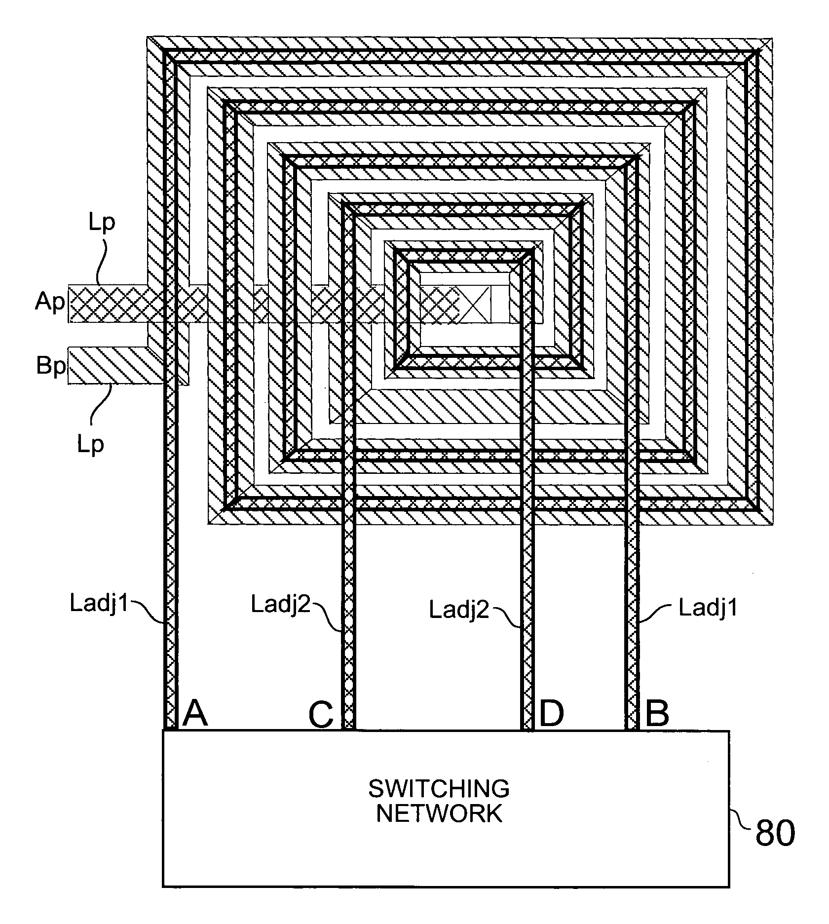
[0014]The present invention provides additional, close loop inductors above and / or below a primary inductor. Each of the closed loop inductors may have its closed loop, i.e. closed current path, selectively broken. When the current path of the close loop inductor is not broken, it can generate an induced current due to an applied current in the primary inductor. This establishes a mutual inductance that alters the primary inductor's impedance, and thus alters its operating point. If the inductance value of the primary inductor is lower than desired, then the closed circuit loop of the secondary inductor may be opened, i.e. broken, in which case it will no longer be able to generate a an induced current and thereby eliminate any loading effects on the primary inductor.

Problems solved by technology

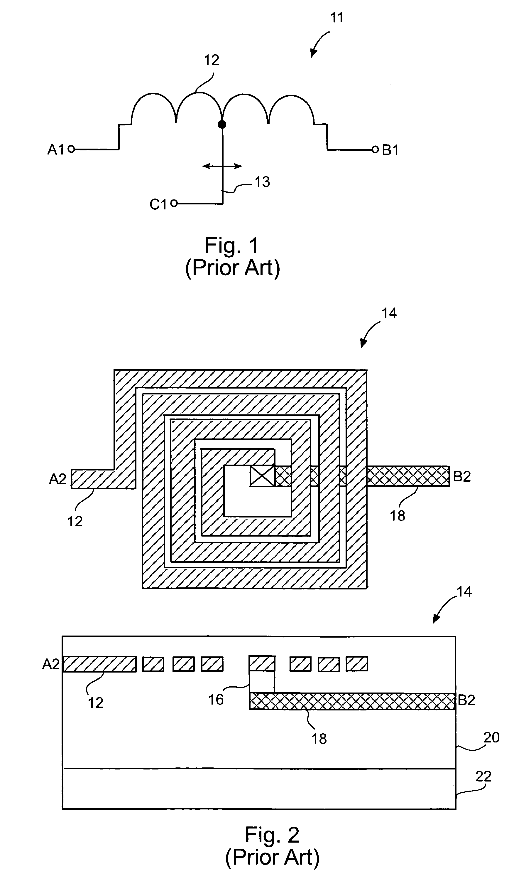
Such a variable inductor 11, however, is not available in integrated circuit technology, where mechanically adjustable armatures are not practical.
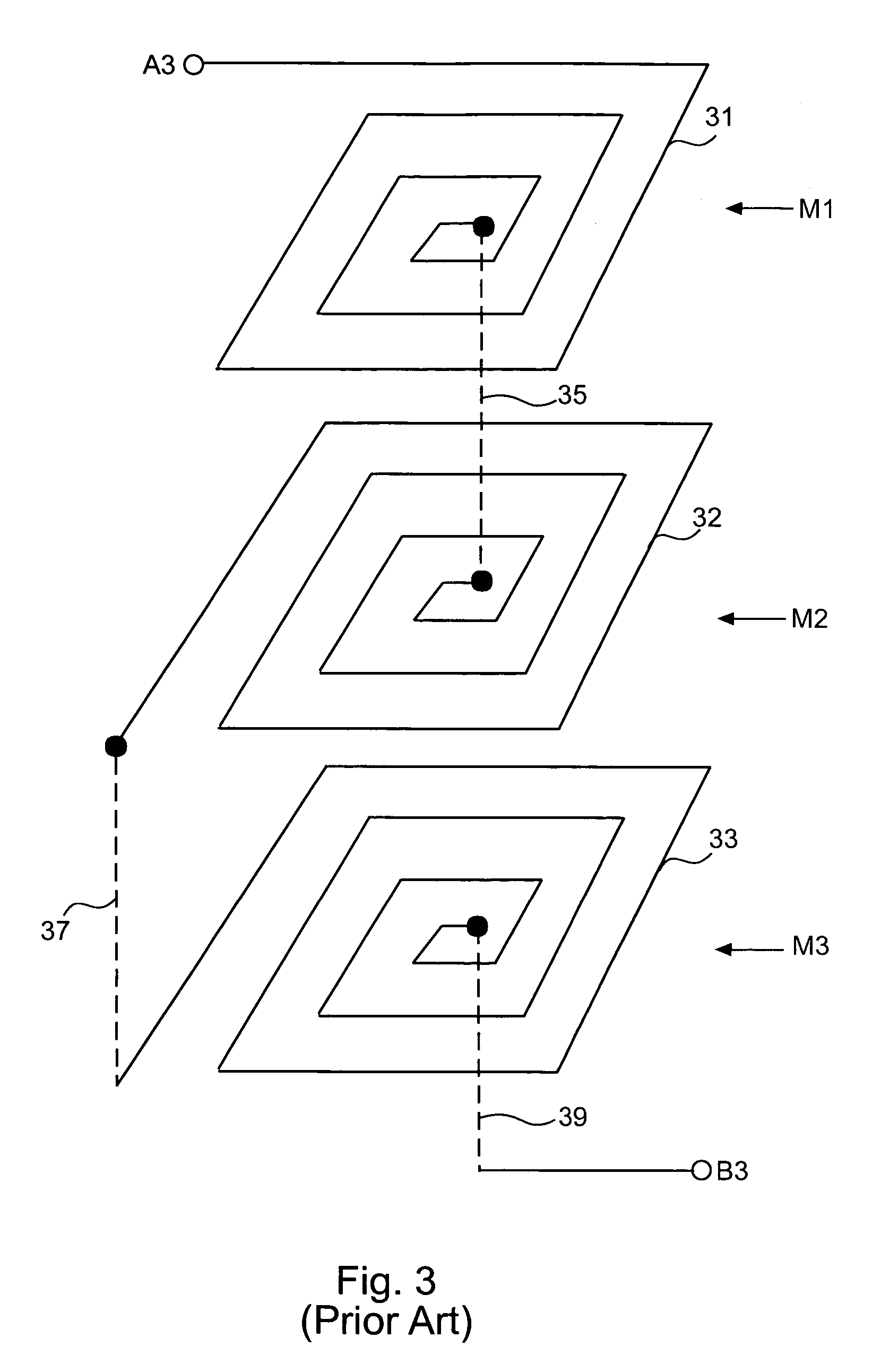
Nonetheless, the large geographic area (which results in possible large amounts of capacitive coupling) as well as the many variations in their manufacturing process still make inductors highly susceptible to variations in their manufacturing process.

Method used


Image

  • Variable inductor technique
  • Variable inductor technique
  • Variable inductor technique

Examples


Embodiment Construction

[0027]An initial attempt toward providing an integrated variable inductor might be to construct an integrated inductor with several fixed tapping points and a switching network, but physical limitations would likely make such a configuration impractical with current manufacturing techniques.

[0028]With reference to FIG. 5, such a configuration may consist of an integrated spiral inductor 40 and a first end point A4 on a first process layer, and a multiplexor 42 producing a variable second end point B4 on a second process layer. In the present case, vias V1 through V4 provide four possible tap points at four distinct locations along spiral 40. Thus, one could conceivable tap spiral 40 at any one of the four tap points producing an inductor of varying length by applying an appropriate selection signal to the control input of multiplexor 42. However, the addition of multiple vias as tap points and circuitry for multiplexor 42 introduces a large amount of parasitic capacitive and inducti...


PUM

PropertyMeasurementUnit
conductiveaaaaaaaaaa
widthaaaaaaaaaa
dielectricaaaaaaaaaa

Abstract

An integrated variable inductor is achieved by placing a second closed-loop inductor immediately above or below a primary inductor. The closed-loop configuration of the second inductor may be broken on-chip by several ways, including use of a transistor to selectively short together both ends of the second inductor. If one wishes to alter the inherent inductance characteristics of the primary inductor, the transistor coupling both ends of the second inductor is actuated. Thus, a current applied to the primary inductor induces a current in the second inductor by inductive coupling. The second current in the second inductor then alters the impedance of the primary inductor by mutual inductance. Thus, the inductance value of the primary inductor is altered. To remove the influence of the second inductor on the primary inductor, the closed-loop configuration of the second inductor is broken.

Description

BACKGROUND OF THE INVENTION[0001]1. Field of the Invention[0002]The present invention is geared toward the field of integrated inductors, and particularly toward the construction of an integrated variable inductor whose inductance value may be adjusted on-chip.[0003]2. Description of the Related Art[0004]Inductors are an integral part of discrete radio frequency, RF, circuitry. Particularly, discrete variable inductors are typically used for tuning purposes.[0005]With reference to FIG. 1, a discrete variable inductor 11 may consist of an inductor coil 12 between two end points (A1 and B1) and a mechanically adjustable armature 13 that may be slid along coil 12. One end 15 of armature 13 contacts coil 12 and the other end C1 provides an electrical contact for producing the desired variable inductance. The inductance value, L, of an inductor is dependent upon (among other factors) the number of windings in the coil between to electrical contact points, and one may adjust the number of...

Claims


Application Information

Patent Timeline
Patent Type & Authority Patents(United States)
IPC IPC(8): H01F5/00
CPCH01F17/0013H01F21/12H01L23/5227H01L27/08H01F17/0006H01F2021/125H01L2924/0002H01L2924/3011H03J2200/35H01L2924/00
Inventor HARGROVE, MICHAELPETROSKY, JOSEPH
Owner 138 EAST LCD ADVANCEMENTS LTD
Learn More