Methods and systems for protection from over-stress

a technology of overstress and methods, applied in emergency protective circuit arrangements, instruments, heat measurement, etc., can solve problems such as circuit failure and mosfet failure, and achieve the effect of facilitating switching of semiconductor devices

Active Publication Date: 2009-10-27
INFINEON TECH AG
View PDF7 Cites 9 Cited by
  • Summary
  • Abstract
  • Description
  • Claims
  • Application Information

AI Technical Summary

Problems solved by technology

Over-stress can often be caused by overload or faulted operating conditions and can impart, for example, thermo-mechanical stress on an integrated circuit, which can eventually lead to failure of the circuit.
For example, if a MOSFET device operates at a temperature above its maximum critical temperature, electrical over-stress can cause the MOSFET to eventually fail.

Method used


Image

  • Methods and systems for protection from over-stress
  • Methods and systems for protection from over-stress
  • Methods and systems for protection from over-stress

Examples


Embodiment Construction

[0008]The present invention will now be described with respect to the accompanying drawings in which like numbered elements represent like parts. The figures and the accompanying description of the figures are provided for illustrative purposes.

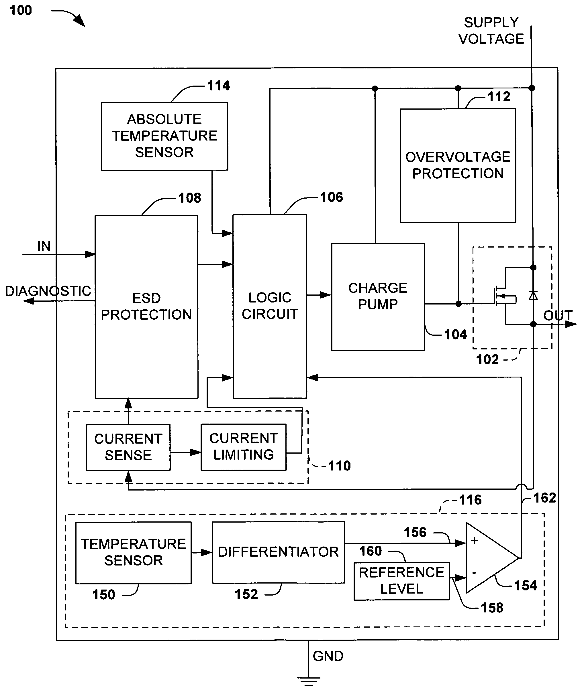
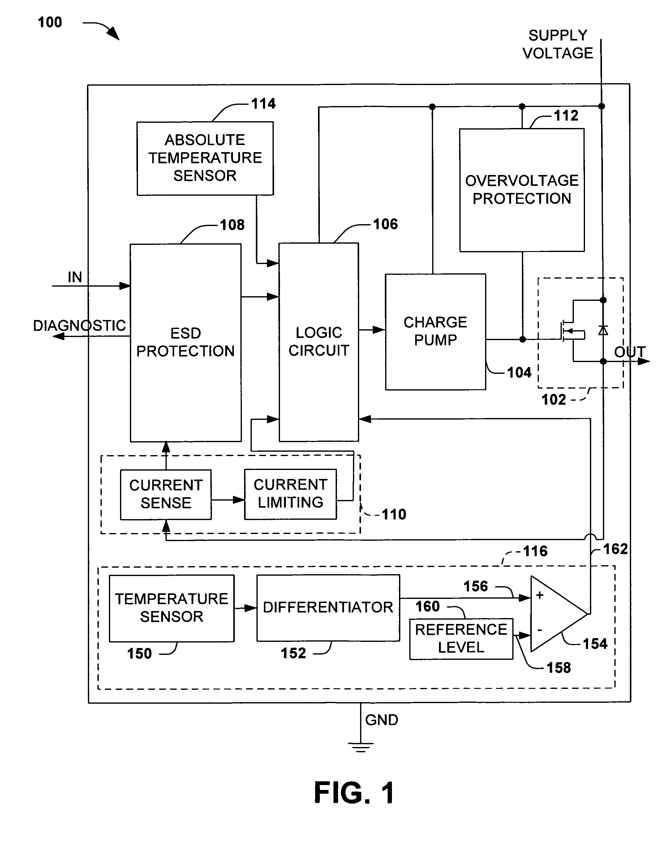
[0009]FIG. 1 shows one embodiment of a circuit 100 capable of providing protection against electrical over-stress and other protection functions. The illustrated circuit 100 relates to a power switch that combines MOS power and MOS logic circuitry. The circuit 100 can be a monolithic single- or multi-channel switch, or a single channel switch using chip-on-chip technology. Other suitable arrangements could also be utilized.

[0010]As shown, the circuit 100 includes a semiconductor device 102 (e.g., a vertically structured N-channel power transistor), a charge pump 104 for high side operation, and a logic circuit 106 for facilitating various protection functions. Although the illustrated circuit shows a semiconductor device 102 as a vertically s...


PUM

PropertyMeasurementUnit
temperatureaaaaaaaaaa

Abstract

One embodiment of the invention relates to a circuit for over-stress protection. The circuit includes a temperature rate sensor configured to monitor the temperature of a semiconductor device during a first state. The circuit is further configured to selectively switch the semiconductor device from the first state to a second state if the temperature increases at a rate that has a predetermined relationship with a temperature rate function. Other methods and systems are also disclosed.

Description

FIELD OF THE INVENTION[0001]The present invention relates generally to semiconductor devices, and more specifically to methods and systems for protection from over-stress.BACKGROUND OF THE INVENTION[0002]Over-stress can often be caused by overload or faulted operating conditions and can impart, for example, thermo-mechanical stress on an integrated circuit, which can eventually lead to failure of the circuit.[0003]For example, if a MOSFET device operates at a temperature above its maximum critical temperature, electrical over-stress can cause the MOSFET to eventually fail. Because electrical over-stress can affect the reliability of practically all integrated circuits to some extent, improvements in over-stress detection and protection are always ongoing. As such improvements can extend the lifetime of integrated circuits and devices connected thereto, these improvements are a valuable contribution to the marketplace.SUMMARY OF THE INVENTION[0004]One embodiment relates to a method f...

Claims


Application Information

Patent Timeline
Patent Type & Authority Patents(United States)
IPC IPC(8): G01K7/00G01K3/00H02H5/04
CPCG06F1/206H01L23/34H01L2924/0002H01L2924/00
Inventor BEIER, ROBERT CARLNOTARANTONIO, RAYMOND JOSEPH
Owner INFINEON TECH AG
Why Eureka
Try Eureka