Printed wiring board and method for manufacturing the same

a printing method and wiring board technology, applied in the direction of etching metal masks, semiconductor/solid-state device details, insulating substrate metal adhesion improvement, etc., can solve the problems of wasteful procedures, inconvenient manufacturing methods, and inability to build up an odd number of conductive layers

Inactive Publication Date: 2009-11-03
IBIDEN CO LTD
View PDF51 Cites 26 Cited by
  • Summary
  • Abstract
  • Description
  • Claims
  • Application Information

AI Technical Summary

Benefits of technology

[0028]Further, conductive layers can be built up on the upper side and lower side of the central insulating layer efficiently.
[0079]Further, since the areas to be occupied by the interconnecting through holes and solder balls are narrowed to afford extra spaces on the surface of the insulating substrate, conductor circuits and the like can be formed on such extra spaces, enabling high densification of surface packaging on the insulating substrate.

Problems solved by technology

However, the conventional method of manufacturing printed wiring boards as described above is not suitable for building up an odd number of conductive layers, although it can build up an even number of conductive layers efficiently.
Thus, the conventional method requires wasteful a procedure and is an extremely inefficient manufacturing method.
Further, the insulating layers formed are too thick to meet the purpose of achieving downsizing of printed wiring boards.
Accordingly, the method requires intricate procedures of defining through holes.
Particularly, with the reduction in the size of the interconnecting through holes, it is becoming difficult to carry out accurate registration of the through holes.
However, the connecting circuits which occupy a large surface area are a hindrance in achieving high-density packaging on the substrate surface.
Further, large amounts of electric currents must fed in and out through the external connecting terminals.

Method used


Image

  • Printed wiring board and method for manufacturing the same
  • Printed wiring board and method for manufacturing the same
  • Printed wiring board and method for manufacturing the same

Examples


first embodiment

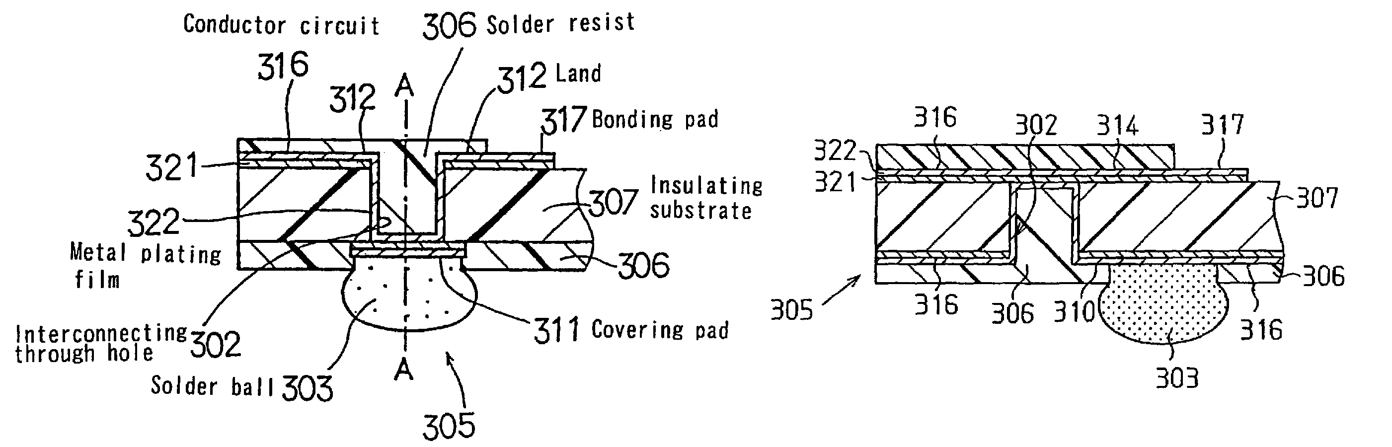
[0180]The printed wiring board of the embodiment according to the first aspect of the invention will be explained referring to FIGS. 1 to 9.

[0181]The printed wiring board 41 of the first embodiment has three conductive layers 11 to 13 which are built up via insulating layers 21 to 23 respectively, as shown in FIG. 1. The conductive layers 11 to 13 are electrically connected to one another by interconnecting through holes 31 and 32.

[0182]The first conductive layer 11 is a component connecting layer on which an electronic component 61 is mounted and leads electric currents in and out of the component 61.

[0183]The second conductive layer 12 is an electric current transmitting layer for transmitting internal electric currents of the printed wiring board 41.

[0184]The third conductive layer 13 is an external connecting layer for connecting external connecting terminals 7 for leading electric currents in and out of the printed wiring board 41. The surface of the third and outermost conduct...

second embodiment

[0204]The printed wiring board of the second embodiment has five conductive layers 11 to 15 which are built up as shown in FIG. 10.

[0205]The first conductive layer 11 is a component connecting layer on which an electronic component 61 is mounted and leads electric currents in and out of the component 61.

[0206]The second to fourth conductive layers 12 to 14 are electric current transmitting layers for transmitting internal electric currents of the printed wiring board 42.

[0207]The fifth conductive layer 15 is an external connecting layer for connecting external connecting terminals 7 for leading electric currents in and out of the printed wiring board 42. The surface of the fifth conductive layer 15 is covered with the fifth and outermost insulating layer 25 with the external connecting terminals 7 being exposed.

[0208]When a printed wiring board 42 of this embodiment is manufactured, conductive layers 13 and 14 and interconnecting through holes 33 are formed in the third and central ...

third embodiment

[0213]The printed wiring board of the embodiment according to the second aspect of the invention will be explained referring to FIG. 11.

[0214]As shown in FIG. 11, the printed wiring board 101 of the third embodiment has an internal insulating substrate 116 having on each side a conductor circuit 115, an internal insulating layer 117 laminated on the surface of the internal insulating substrate 116 and an external insulating layer 118 laminated on the internal insulating layer 117. Each internal insulating layer 117 has on the surface an internal conductor circuit 125, while each external insulating layer 118 has on the surface an external conductor circuit 135.

[0215]The internal insulating layer 117 is of a glass cloth-reinforced prepreg, whereas the external insulating layer 118 is of a resin.

[0216]The internal insulating layer 117 is a prepreg prepared by impregnating a glass cloth with an epoxy resin, and the external insulating layer 118 is an epoxy resin.

[0217]Next, the printed...


PUM


Abstract

In a printed wiring board, an odd number (n) of conductive layers (11-13) and insulating layers (21-23) are alternately laminated upon another. The first conductive layer (11) is constituted as a parts connecting layer and the n-th conductive layer (13) is constituted as an external connecting layer which is connected to external connecting terminals (7). The second to (n−1)-th conductive layers (12) are constituted as current transmitting layers for transmitting internal currents. The surface of the n-th conductive layer (13) is coated with the outermost n-th insulating layer (23) in a state where the external connecting terminals (7) are exposed on the surface. It is preferable to constitute the initial insulating layers of a glass-cloth reinforced prepreg and the external insulating layers of a resin.

Description

CROSS REFERENCE[0001]This application is a division of application Ser. No. 09 / 380,994, filed Sep. 13, 1999 now U.S. Pat. No. 7,339,118.TECHNICAL FIELD[0002]The present invention relates generally to a multilayered printed wiring board capable of realizing high-density packaging and a method for manufacturing the same, and particularly to a printed wiring board having an odd number of conductive layers, a printed wiring board having build-up layers formed by using the additive method and the like, a method of forming interconnecting through holes for electrically connecting conductive layers and narrowing the pitch between solder balls for external connection and the interconnecting through holes.BACKGROUND ART[0003]Conventional printed wiring boards include those having conductive layers 911 to 914 built up successively, as shown in FIG. 42. The conductive layers 911 to 914 are electrically connected to one another via interconnecting through holes 931 to 933. Insulating layers 921...

Claims


Application Information

Patent Timeline
Patent Type & Authority Patents(United States)
IPC IPC(8): H05K1/16H05K3/00H01L23/12H01L23/498H01L23/50H05K1/11H05K3/28H05K3/34H05K3/38H05K3/46
CPCH01L24/49H05K3/4602H01L23/49822H05K1/114H05K1/113H05K3/429H01L23/50H05K2201/09536H05K2203/0554H05K2201/0394Y10T29/4913H05K3/4697H01L2224/32225H01L2924/01033H01L2924/01029H05K2203/0315H01L2924/15153H01L2924/01028H01L2924/01078H01L2224/49109H01L2924/01006H01L24/48H05K1/021H01L2924/01047H05K2201/09472H01L2224/48227H01L2924/01004H01L2924/01005H01L2924/01079H05K3/3457H01L2924/15311H05K2201/0959H01L2924/12041H05K2201/09509H05K2201/09527H01L2924/01082H05K3/4652H05K3/28H01L2924/1532Y10T29/49126H05K2201/0355H05K3/385H01L2924/1517H05K3/0035H01L2924/07802H01L2224/32245H01L2224/73265H01L2924/014H01L2224/48091H01L2924/01074H05K2203/1581H01L2924/00014H01L2924/00H01L2924/00012H01L24/73H01L2924/12042H01L2924/181H01L2924/351H01L2224/45099H01L2224/05599H01L23/12
Inventor TAKADA, MASARUMINOURA, HISASHITSUKADA, KIYOTAKAKOBAYASHI, HIROYUKIKONDO, MITSUHIRO
Owner IBIDEN CO LTD
Why Eureka
Try Eureka