Differential alternating phase shift mask optimization

a technology of alternating phase shift and mask optimization, which is applied in the field of mask manufacturing, can solve the problems of not always presenting the best altpsm design for optical proximity correction (opc, unfavorable tradeoffs), and achieve the effects of optimizing balance, efficiency and accuracy, and improving the opc performance of localized altpsm designs

Inactive Publication Date: 2009-11-10
GLOBALFOUNDRIES INC
View PDF5 Cites 4 Cited by
  • Summary
  • Abstract
  • Description
  • Claims
  • Application Information

AI Technical Summary

Benefits of technology

[0008]In particular, it is an object of the present invention to provide a method of designing altPSMs that strikes an optimized balance between the efficiency and accuracy benefit of global design solutions and the improved OPC performance of localized altPSM designs.
[0009]Another object of the present invention is to extend the benefits of the optimization of global and localized design solutions to other lithographic mask features used to enhance resolution of critical width features, such as sub-resolution assist features (SRAF).

Problems solved by technology

One of the major challenges in generating an altPSM layout is to create manufacturable and lithographically viable phase shapes without introducing undue layout conflicts, and without introducing optical proximity errors.
While these global approaches to altPSM design avoid costly and often error prone iterative phase legalization, they do not always present the best altPSM design for optical proximity correction (OPC).
Extraneous phase shapes employed in the global PSM design approach add to the OPC complexity and may result in unfavorable tradeoffs with critical phase edges that directly impact the patterning of primary layout shapes.

Method used


Image

  • Differential alternating phase shift mask optimization
  • Differential alternating phase shift mask optimization
  • Differential alternating phase shift mask optimization

Examples


Embodiment Construction

)

[0033]In describing the preferred embodiment of the present invention, reference will be made herein to FIGS. 1-12 of the drawings in which like numerals refer to like features of the invention.

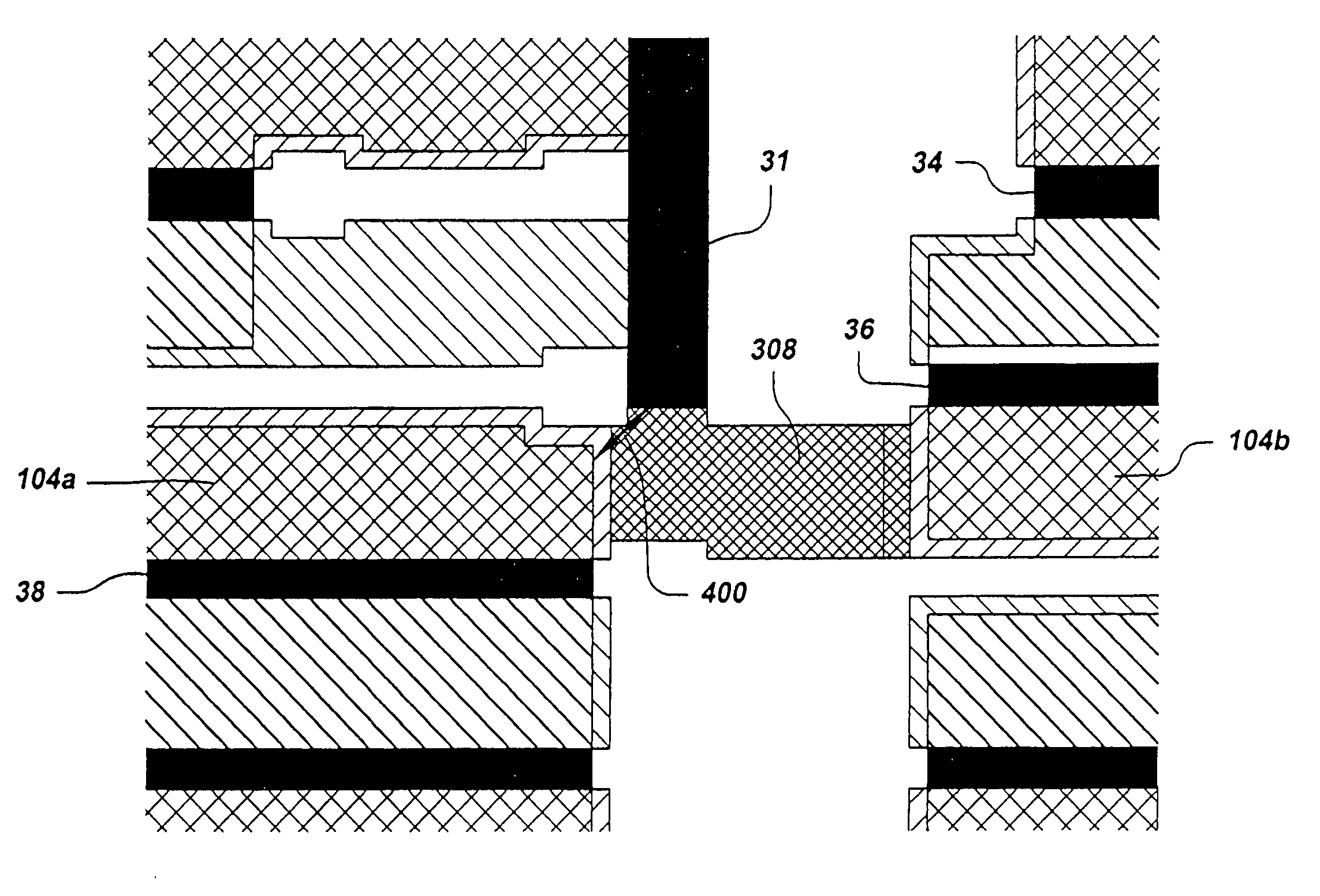
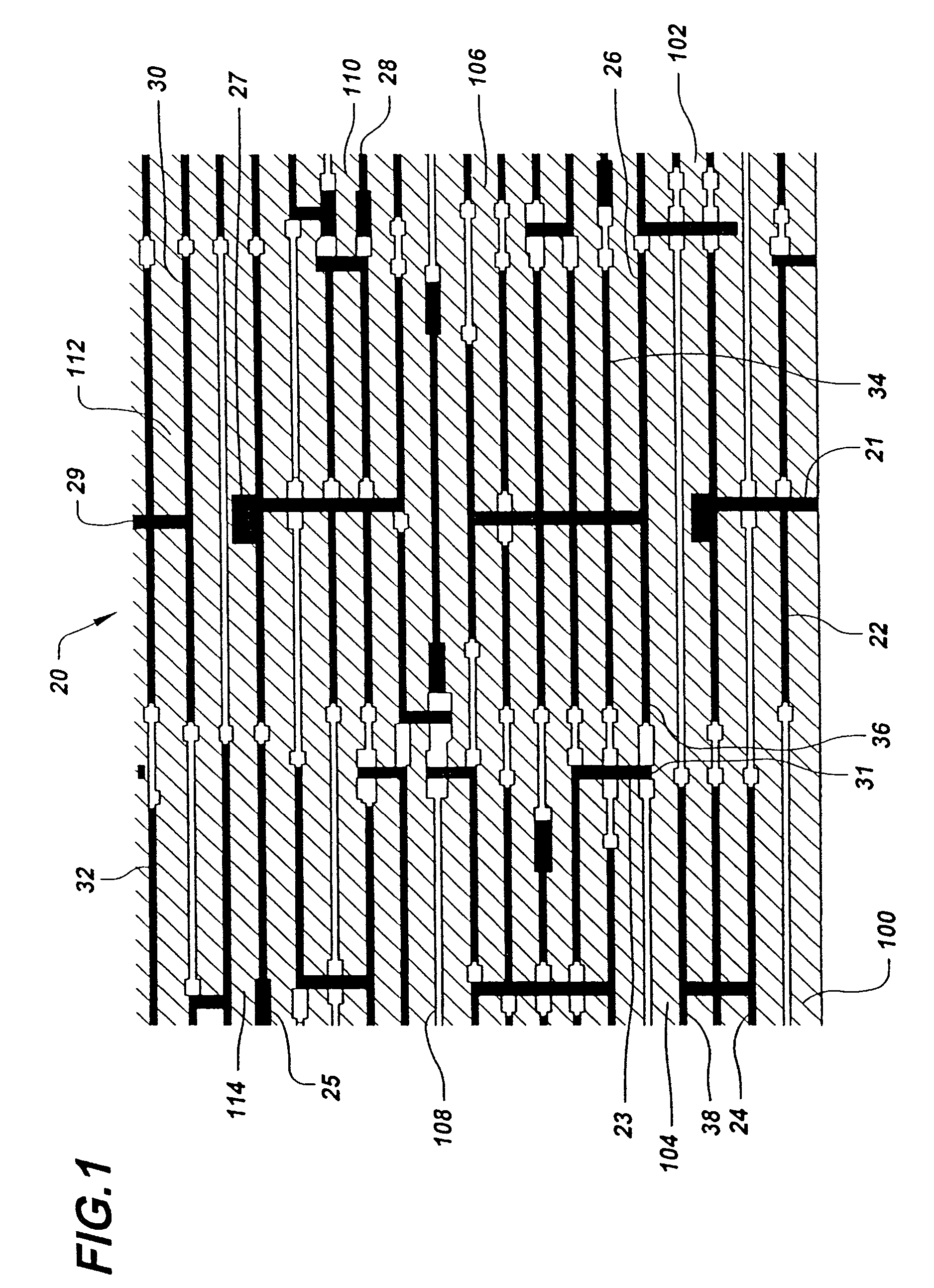
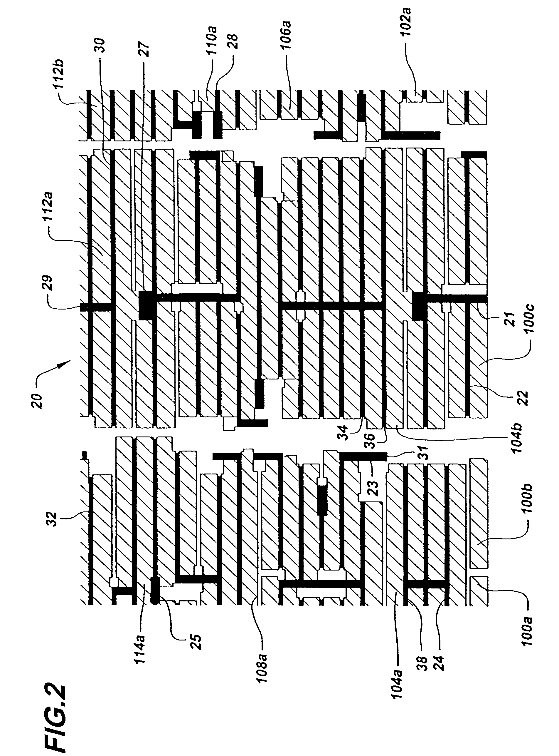
[0034]In one preferred embodiment of the present invention, there is initially designed a global altPSM design, based on the teachings of the aforementioned U.S. Pat. No. 7,229,722, the disclosure of which is hereby incorporated by reference. As shown in FIG. 1, critical width segments of an integrated circuit layout 20, for example those identified as even numbered segments 22-38, have a plurality of essentially parallel segments oriented horizontally. As used herein, the term critical segment refers to segments, or portions thereof, that have a critical dimension, i.e., a dimension smaller than the smallest dimension that the lithographic system can create with adequate dimensional control on the resist layer. Also in FIG. 1 are non-critical segments of the integrated circuit layout, for e...


PUM


Abstract

A method of designing a mask for projecting an image of an integrated circuit design in lithographic processing, wherein the integrated circuit layout has a plurality of segments of critical width. The method comprises creating a first mask design by aligning mask features used to assist in projecting critical width segments with the critical width segments of the integrated circuit design, such that the first mask design meets predetermined manufacturability design rules, and creating a second mask design by aligning mask features with the critical width segments of the integrated circuit design, such that the second mask design meets predetermined lithographic design rules in regions local to the critical width segments. The method then includes identifying design features of the second mask design that violate the predetermined manufacturability design rules, and then creating a third mask design derived from the second mask design wherein the mask features of the second mask design that violate the predetermined manufacturability rules are selectively replaced by mask features from the first mask design so that the third mask design meets the predetermined manufacturability design rules. By way of example, the mask features used to assist in projecting critical width segments may comprise alternating phase shifting regions or sub-resolution assist features.

Description

BACKGROUND OF THE INVENTION[0001]1. Field of the Invention[0002]The present invention is directed to the manufacture of masks used in the lithographic production of integrated circuits and, in particular, to the manufacture of resolution enhancement technique (RET) enhanced masks, more particularly, to the automated and optimized conversion of IC layouts to RET mask designs[0003]2. Description of Related Art[0004]As an alternative to chrome on glass (COG) masks used in the lithographic production of integrated circuits, alternating phase shifting masks (altPSMs) have been employed in order to increase the resolution of the critical active area patterns projected. Such increased resolution enables smaller line widths and tighter pitches to be exposed on the resist and consequently etched into or deposited on the wafer substrate. The critical dimension (CD) of the system is the smallest dimension that the lithographic system can create with adequate dimensional control on the resist l...

Claims


Application Information

Patent Timeline
Patent Type & Authority Patents(United States)
IPC IPC(8): G06F17/50
CPCG03F1/144G03F1/29G03F1/30
Inventor LIEBMANN, LARS W.BAUM, ZACHARY
Owner GLOBALFOUNDRIES INC
Why Eureka
Try Eureka