Integrated connection arrangements

a technology of integrated connection and connection arrangement, which is applied in the direction of semiconductor devices, semiconductor/solid-state device details, electrical devices, etc., can solve the disadvantage of copper wiring, achieve the effects of reducing the thickness of the conductive layer, increasing the current density, and reducing the current-carrying capacity

Active Publication Date: 2009-11-17
INFINEON TECH AG
View PDF35 Cites 49 Cited by
  • Summary
  • Abstract
  • Description
  • Claims
  • Application Information

AI Technical Summary

Benefits of technology

[0014]A via metallization stratum may be arranged under a metallization stratum with the connections, adding spatial steps, such as a dielectric having an oxide, a material having a relative permittivity of less than 3.7, a fluorosilicate glass (FSG), a polyimide or silicon nitride. Steps in the dielectric may lead to a local reduction of the thickness of the conductive layer, and thus to a reduced current-carrying capacity. If metallizations are deposited at these steps, then the layer thickness decreases at the steps on account of process effects to values of, for example, approximately 50% of the layer thickness in planar regions. This, in turn, has the effect that the current density increases at the step. Therefore an increase in current density results due to a geometry or thickness narrowing and hence a locally increased current density.

Problems solved by technology

An obstacle to underlaying the bonding pad with copper over a whole area is the fact that a copper wiring is disadvantageous on account of the mechanical stability under the region of the aluminum pads which is used for the connection and for testing.

Method used


Image

  • Integrated connection arrangements
  • Integrated connection arrangements
  • Integrated connection arrangements

Examples


Embodiment Construction

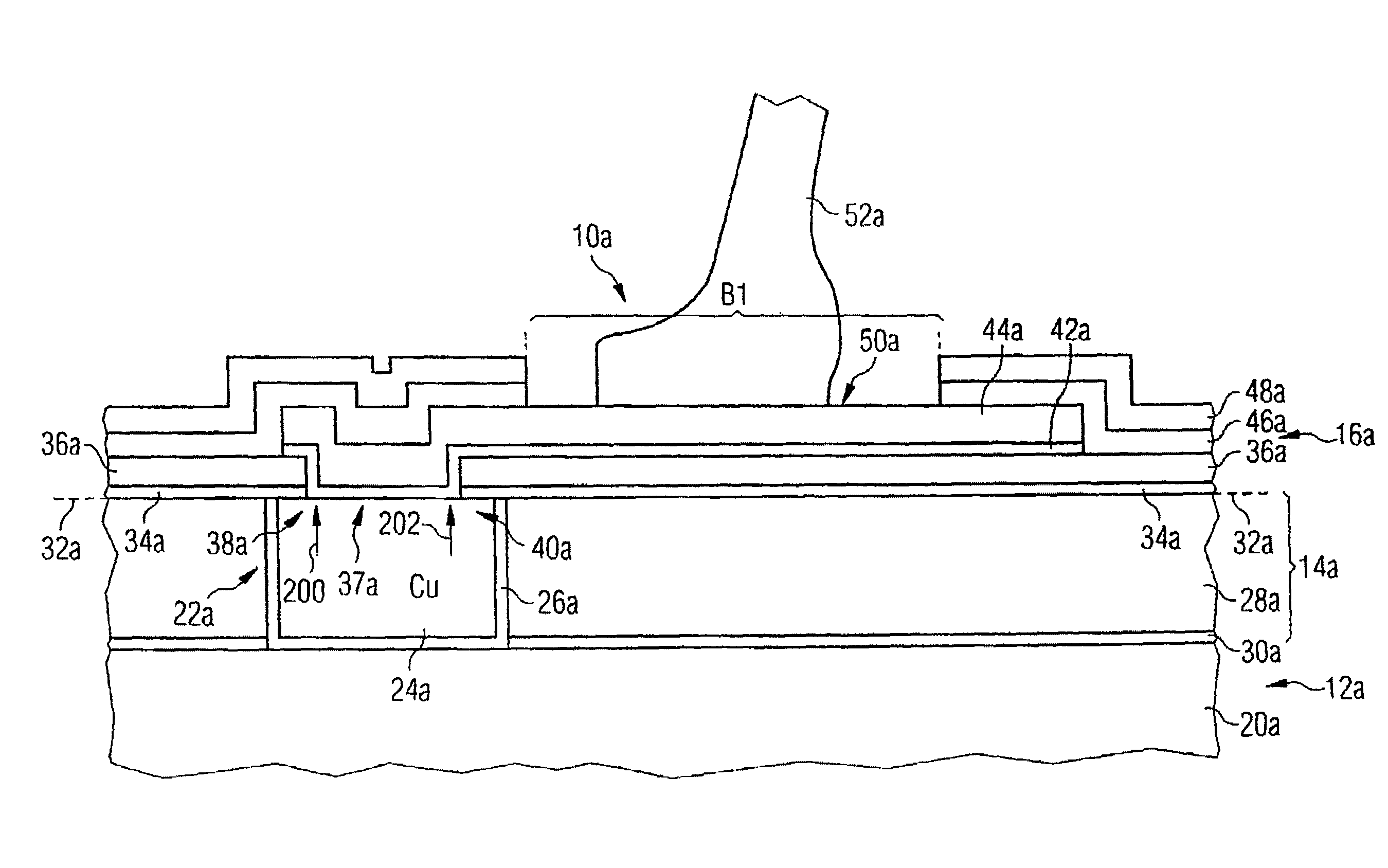
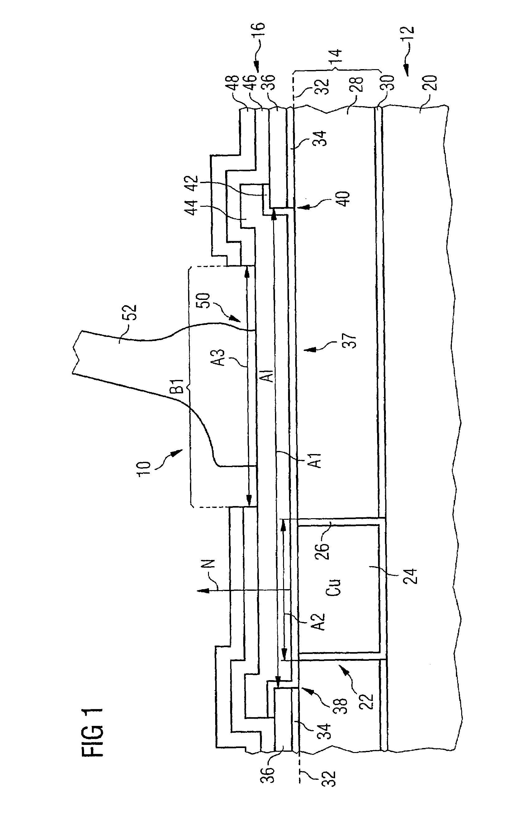
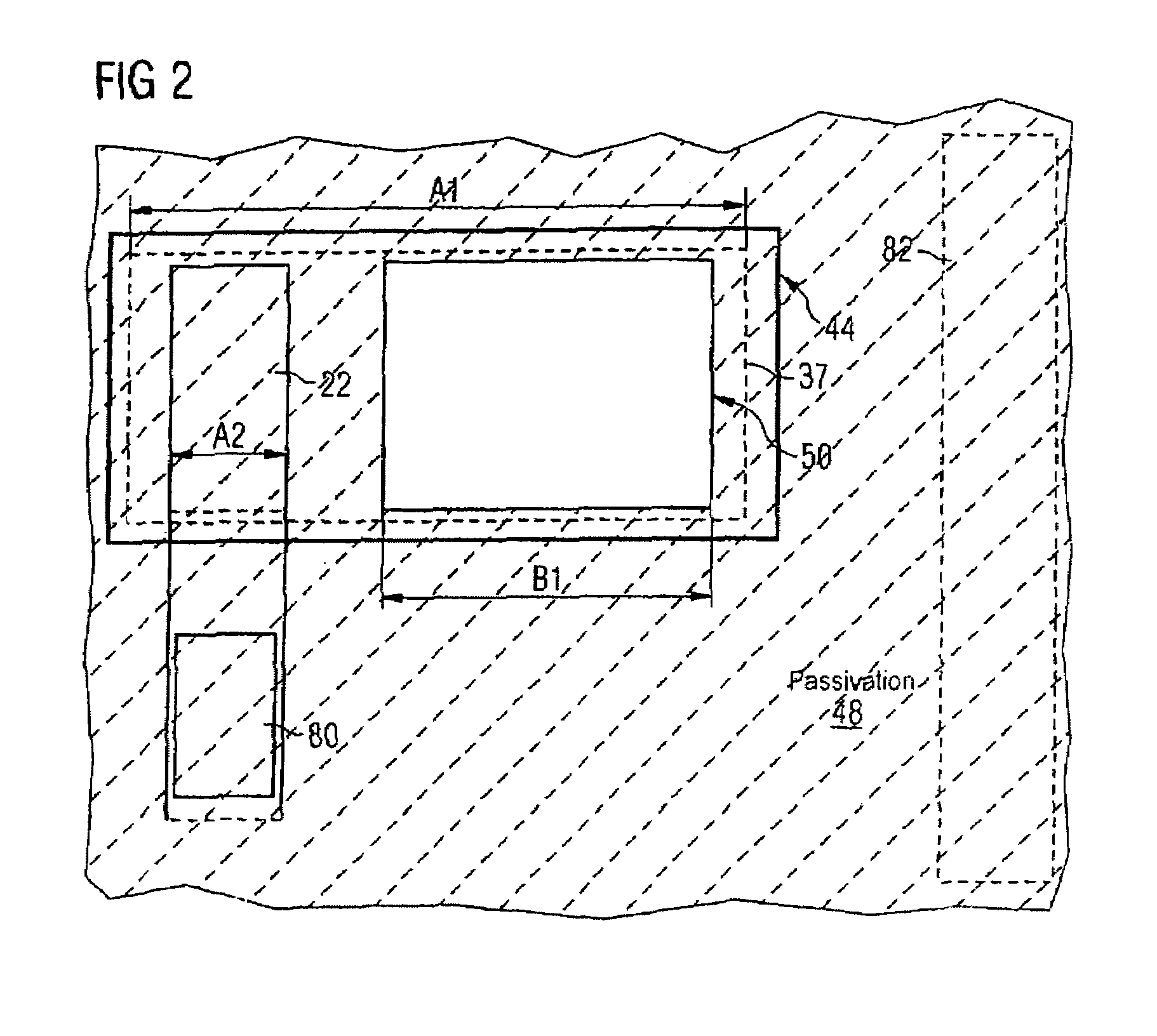
[0041]FIG. 1 shows an integrated circuit arrangement 10 having a substrate (not illustrated), such as a silicon substrate, with multiple integrated semiconductor components. The integrated circuit arrangement 10 includes metallization strata 12, 14 and 16. The metallization stratum 12 includes copper vias each having a copper core 18, and an electrically conductive barrier layer. The electrically conductive barrier layer may be tantalum, tantalum nitride, titanium nitride or a combination thereof. The barrier layer may provide a liner or a diffusion barrier that promotes adhesion and orientation during copper deposition. Vertical conductive structures of the metallization stratum 12 are embedded in an insulation material 20. The insulation material 20 may be silicon dioxide.

[0042]The metallization stratum 19 includes multiple conductive structures, such as vertical conductive structures and interconnects such as interconnect 22 having a copper core 24. The metallization stratum 14 i...


PUM


Abstract

A connection arrangement having an outer conductive structure arranged at least partly or completely in a cutout of an electrical insulation layer is provided. An inner conductive structure is arranged at the bottom of the cutout on one side of the insulation layer. The inner conductive structure adjoins the outer conductive structure in a contact zone. A contact area is arranged at the outer conductive structure on the other side of the cutout. The contact zone and the contact area do not overlap. The bottom of the cutout is arranged to overlaps at least half of the contact area, to provide a step in the insulation layer at the edge of the cutout outside a main current path between the contact area and the inner conductive structure.

Description

PRIORITY AND CROSS REFERENCE TO RELATED APPLICATION[0001]This application is a continuation of International Application No. PCT / EP2004 / 051569 filed Jul. 21, 2004, which claims priority to German application 103 37 569.4, filed Aug. 14, 2003, both of which are incorporated in their entirety by reference herein.BACKGROUND OF THE INVENTION[0002]1. Field of the Invention[0003]The invention relates to an integrated connection arrangement, and in particularly to semiconductor components having a substrate, an outer conductive structure remote from the substrate.[0004]2. Description of the Related Art[0005]An integrated circuit arrangement may include an outer conductive structure having a bonding pad with a bonding zone and a test zone. A metallization stratum having vias may be arranged between two metallization strata with interconnects. Current flows in the vias normal to or counter to a normal direction to a main area, but not parallel to the main area or transversely with respect to...

Claims


Application Information

Patent Timeline
Patent Type & Authority Patents(United States)
IPC IPC(8): H01L23/48H01L21/4763H01L23/52H01L29/40H01L23/485H01L23/532
CPCH01L23/53228H01L24/03H01L24/05H01L24/48H01L2924/01068H01L2924/01019H01L2924/00014H01L2924/30105H01L2924/19043H01L2224/02166H01L2224/0401H01L2224/04042H01L2224/05073H01L2224/05166H01L2224/05181H01L2224/05553H01L2224/05554H01L2224/05567H01L2224/05624H01L2224/48463H01L2924/01002H01L2924/01004H01L2924/01005H01L2924/01006H01L2924/01013H01L2924/01014H01L2924/0102H01L2924/01022H01L2924/01029H01L2924/01032H01L2924/01033H01L2924/01061H01L2924/01073H01L2924/01075H01L2924/01079H01L2924/01082H01L2924/014H01L2924/04941H01L2924/04953H01L2924/05042H01L2924/14H01L2224/45099
Inventor DREXL, STEFANGOEBEL, THOMASHELNEDER, JOHANNHOMMEL, MARTINAKLEIN, WOLFGANGKORNER, HEINRICHMITCHELL, ANDREASCHWERD, MARKUSSECK, MARTIN
Owner INFINEON TECH AG
Why Eureka
Try Eureka