Unpowered switch and bleeder circuit

a bleeder circuit and switch technology, applied in the field of switches, can solve the problems of unpowered solid-state switches, unpowered rf switches capable of unpowered operation using integrated circuits, unpowered solid-state switches including non-linear elements, and rectification of rf signals, so as to improve switch isolation and linearity, improve the effect of voltage and improve the voltag

Active Publication Date: 2009-11-17
PSEMI CORP
View PDF36 Cites 60 Cited by
  • Summary
  • Abstract
  • Description
  • Claims
  • Application Information

AI Technical Summary

Benefits of technology

[0014]As described above, in one exemplary embodiment, a novel bleeder circuit may be operatively coupled to each of the control lines C1, C1x, C2, and C2x, and to ground. For a POWERED-STATE condition (i.e., operating power is supplied to the switch), in one embodiment, a bleeder circuit provides an OPEN connection (i.e., high-impedance connection) between a control line and ground, thereby allowing the selected control voltages to control the switch and shunt transistors. For the UNPOWERED-STATE condition (i.e., switch circuit is not provided with operating power), in one embodiment, a bleeder circuit provides a CLOSED connection (i.e., low-impedance) between a control line and ground, thereby setting the switch and shunt transistors to the desired UNPOWERED-STATE condition. The bleeder circuits may be incorporated as components of the control circuit, or the bleeder circuits may comprise separate components. The bleeder circuits prevent rectification of RF signals and undesired bias conditions from detrimentally affecting the performance of the RF switches when placed in the UNPOWERED-STATE.
[0017]For some embodiments of the bleeder circuit described above, one or more of the transistors DP1, DP2 and DN1 may each be replaced by a plurality of similar transistors in series. The use of transistors in series is a method for increasing the voltages that can be employed.
[0018]Persons skilled in the arts of designing RF circuits will understand that a plurality of D-E RF switches as described above may be incorporated in a combined circuit known as “cascaded series-shunt pairs.” For example, the output of a first D-E RF switch may be coupled to the input of a second D-E RF switch, the output of the second D-E RF switch may be coupled to the input of a third D-E RF switch, etc., until a last D-E RF switch is coupled to an RF common node or other final output for the combined circuit. Likewise, a plurality of E-D switches may be incorporated into a combined circuit of this type. Such combined circuits are referred to herein as “cascaded” circuits. The use of cascaded circuits allows for improvements in switch performance, such as improvements in switch isolation and linearity.

Problems solved by technology

A challenge associated with designing RF switches capable of unpowered operation using integrated circuits arises from the fact that a transistor generally requires non-zero bias levels for proper operation.
Further, unpowered solid-state switches include non-linear elements.
These can cause rectification of RF signals and undesired bias conditions.
Although relays can be designed to assume desired default operation when unpowered, relays are bulky, expensive, unreliable, require high current to operate, and have limited switching speeds.

Method used


Image

  • Unpowered switch and bleeder circuit
  • Unpowered switch and bleeder circuit
  • Unpowered switch and bleeder circuit

Examples


first embodiment

of a Single-Pole Double-Throw RF Switch

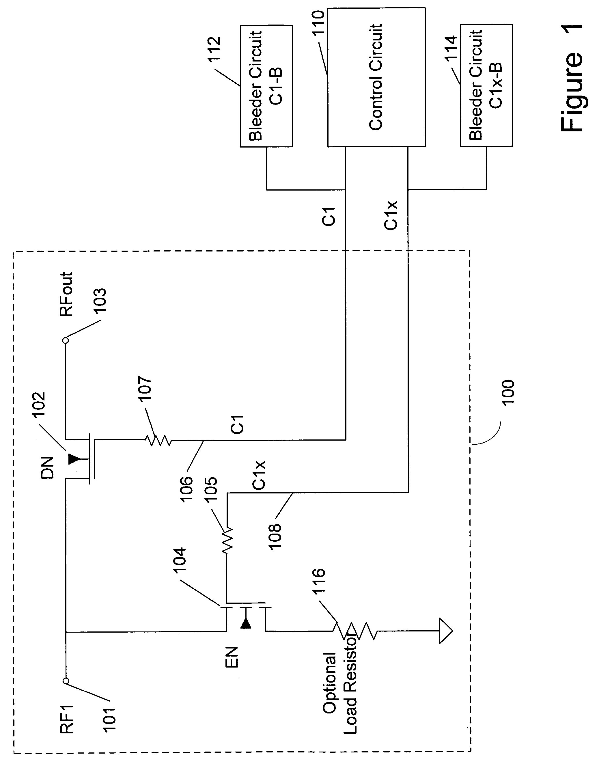
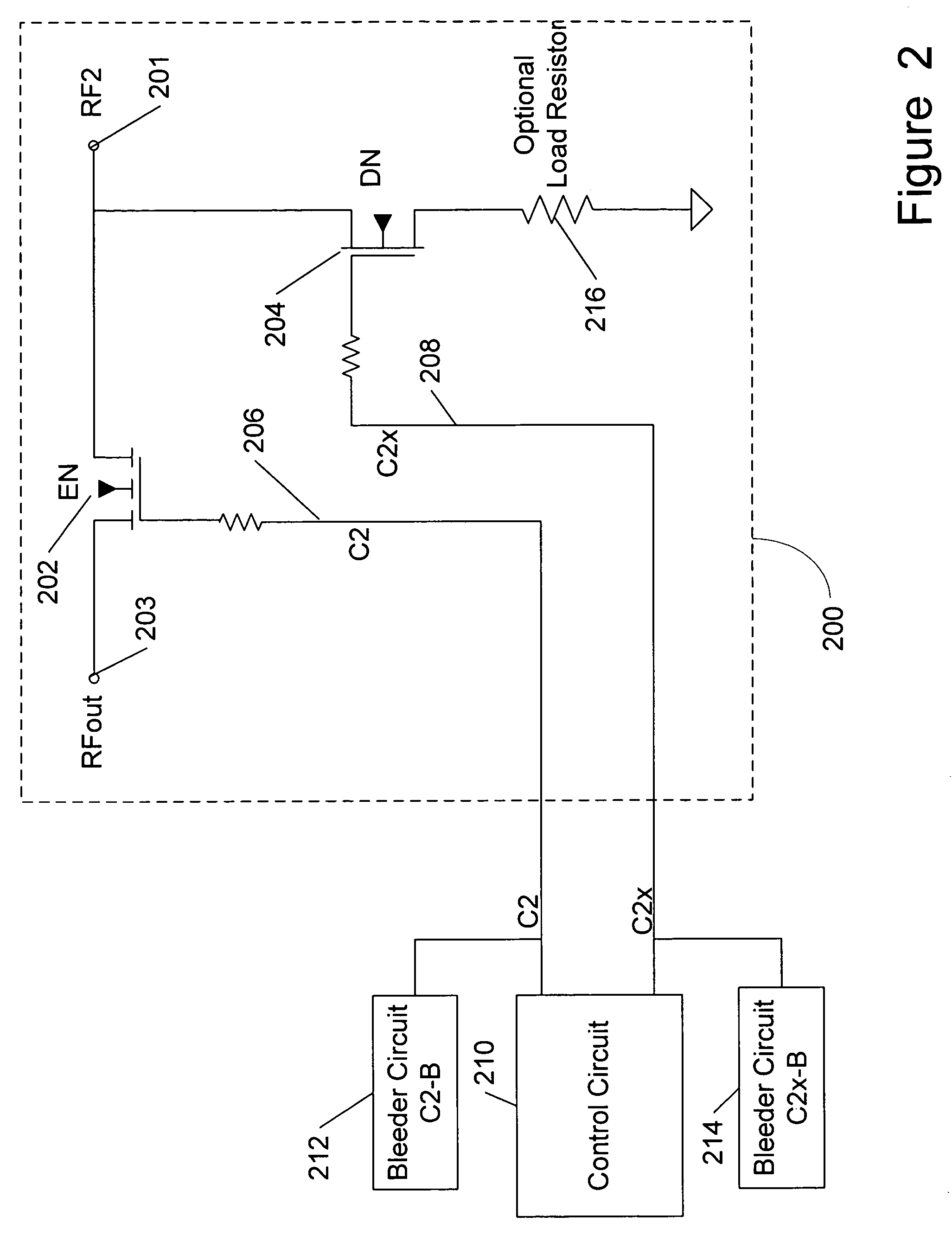
[0065]FIG. 4 schematically illustrates a first embodiment of a single-pole, double-throw (SPDT) RF switch 400 in accordance with the present teachings. In the embodiment shown, the SPDT RF switch 400 includes a D-E RF switch 401 and an E-D RF switch 402. The D-E RF switch 401 is similar to the D-E RF switch 100 described above with reference to the FIG. 1, except that the RF output signal is conveyed to the RF common node 403. Likewise, the E-D RF switch 402 is similar in design to the E-D RF switch 200 described above with reference to FIG. 2, except that the RF output signal is also conveyed to the RF common node 403.

[0066]Referring now to FIG. 5, a control circuit 510 and bleeder circuits 512, 112, 114, 212 and 214 are shown. The control circuit 510 is coupled to provide control voltages to the control lines 502, 106, 108, 206 and 208. The bleeder circuits 512, 112, 114, 212 and 214 are operatively coupled to the control lines 502, 106, 108,...

second embodiment

of a Single-Pole Double-Throw RF Switch

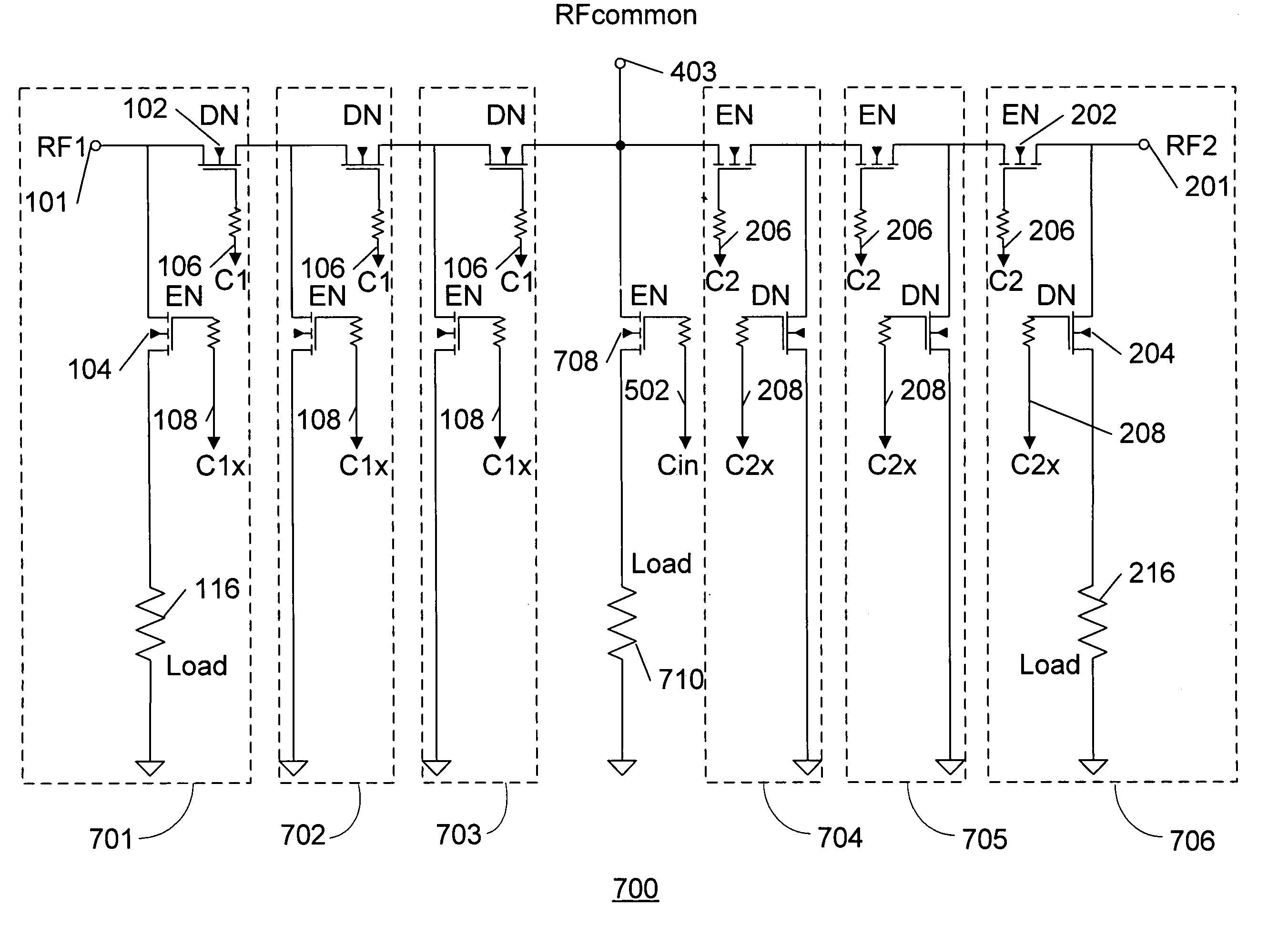
[0070]FIG. 6 schematically illustrates a second embodiment of a single-pole, double-throw (SPDT) RF switch 600 in accordance with the present teachings. The SPDT RF switch 600 includes a first E-D RF switch 601 and a second E-D RF switch 602. The first and second E-D RF switches 601 and 602 are similar to the E-D RF switch 200 described above with reference to FIG. 2, except that the RF output signals are applied to the RF common node 403 in the switch shown in FIG. 6.

[0071]The control voltages provided by the control circuit 510 (FIG. 5) (i.e., control signals C1, C1x, C2 and C2x, respectively) may be conveyed via the control lines 106, 108, 206 and 208 to like control lines 106, 108, 206 and 208, respectively, shown in the FIG. 6, as described above. The control lines 106, 108, 206 and 208 are also coupled to the bleeder circuits 112, 114, 212 and 214, respectively, as shown in FIG. 5.

[0072]For the POWERED-STATE, the SPDT RF switch 600 switch...


PUM


Abstract

A novel RF switch for switching radio frequency (RF) signals is disclosed. The RF switch may comprise both enhancement and depletion mode field-effect transistors (E-FETs and D-FETs) implemented as a monolithic integrated circuit (IC) on a silicon-on-insulator (SOI) substrate. The disclosed RF switch, with a novel bleeder circuit, may be used in RF applications wherein a selected switch state and performance are required when the switch and bleeder circuits are not provided with operating power (i.e., when the switch and bleeder circuits are “unpowered”).

Description

[0001]This application claims the benefit under 35 U.S.C. § 119(e) of U.S. Provisional Application No. 60 / 651,736, filed Feb. 9, 2005, entitled “UNPOWERED SWITCH AND BLEEDER CIRCUIT”, hereby incorporated by reference herein in its entirety; and this application is related to co-pending and commonly owned application Ser. No. 11 / 347,014, filed Feb. 3, 2006, pending, entitled “Symmetrically and Asymmetrically Stacked Transistor Grouping RF Switch”, which is a Continuation-in-Part (CIP) of co-pending and commonly owned U.S. application Ser. No. 10 / 922,135, filed Aug. 18, 2004, entitled “Switch Circuit and Method of Switching Radio Frequency Signals”, pending, which is a continuation of U.S. Pat. No. 6,804,502 issued Oct. 12, 2004, entitled “Switch Circuit and Method of Switching Radio Frequency Signals”, filed Oct. 8, 2002 as application Ser. No. 10 / 267,531, which claims the benefit under 35 U.S.C. § 119(e) of U.S. Provisional Application No. 60 / 328,353, filed Oct. 10, 2001, entitled “...

Claims


Application Information

Patent Timeline
Patent Type & Authority Patents(United States)
IPC IPC(8): H03K17/687
CPCH04B1/48
Inventor KELLY, DYLAN J.KEMERLING, CLINT L.
Owner PSEMI CORP
Why Eureka
Try Eureka