Metastable-resistant phase comparing circuit

a phase comparing circuit and metal-resistant technology, applied in the field of digital phase comparing circuits, can solve the problems of difficult to provide a sufficient amount of delay time, and achieve the effect of reducing delay time, reducing delay time, and ensuring accuracy

Active Publication Date: 2009-11-24
MICRON TECH INC
View PDF1 Cites 3 Cited by
  • Summary
  • Abstract
  • Description
  • Claims
  • Application Information

AI Technical Summary

Benefits of technology

[0012]In light of the above circumstances, an object of the present invention is to provide a phase comparing circuit for reducing the above-described delay time d1 while reliably preventing an erroneous operation of a next circuit connected to the phase comparing circuit.
[0028]In accordance with the present invention, even if a metastable phenomenon occurs in the phase comparing circuit, an erroneous operation of a next circuit connected to the phase comparing circuit can be prevented. Therefore, it is possible to considerably reduce the delay time which is a known measure to handle the metastable phenomenon. Accordingly, the relevant DLL can be operated at a high frequency while providing a sufficient operation margin.

Problems solved by technology

However, in recent years, the operation frequency of DRAMs has increased rapidly, and thus it is difficult to provide a sufficient amount of delay time d1.

Method used


Image

  • Metastable-resistant phase comparing circuit
  • Metastable-resistant phase comparing circuit
  • Metastable-resistant phase comparing circuit

Examples


first embodiment

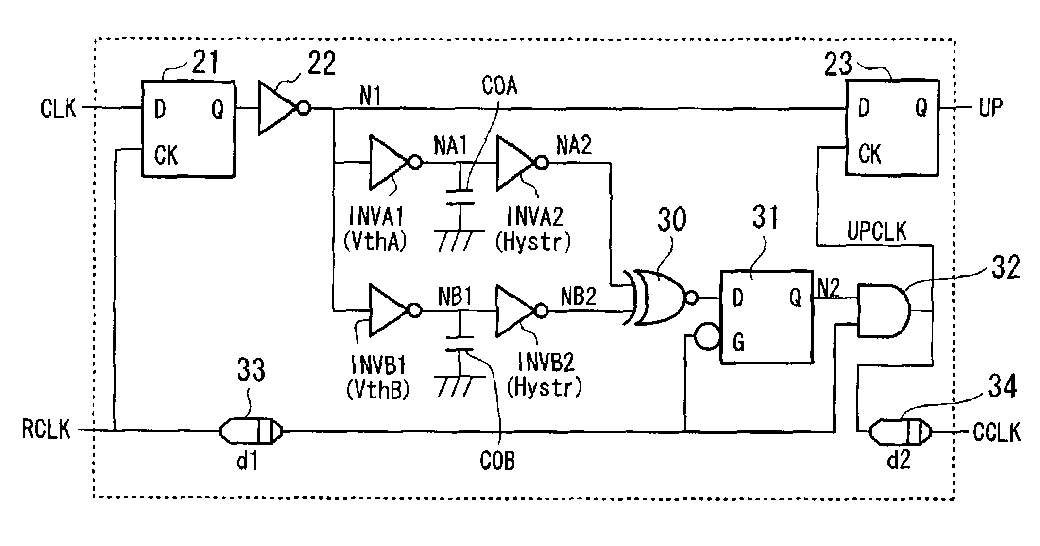
[0037]FIG. 1 is a block diagram showing the structure of a phase comparing circuit as a first embodiment of the present invention. This phase comparing circuit is used in a DLL circuit (refer to FIG. 4).

[0038]In FIG. 1, reference numeral 21 indicates a first D-FF used for reading the external clock signal CLK at the rising edge of the control clock signal RCLK output from the dummy output circuit 9 (see FIG. 4) of the DLL circuit. Reference numeral 22 indicates an inverter used for inverting and outputting the signal output from the D-FF 21. Reference numeral 23 indicates a second D-FF used for reading the signal output from the inverter 22 at the rising edge of a signal UPCLK.

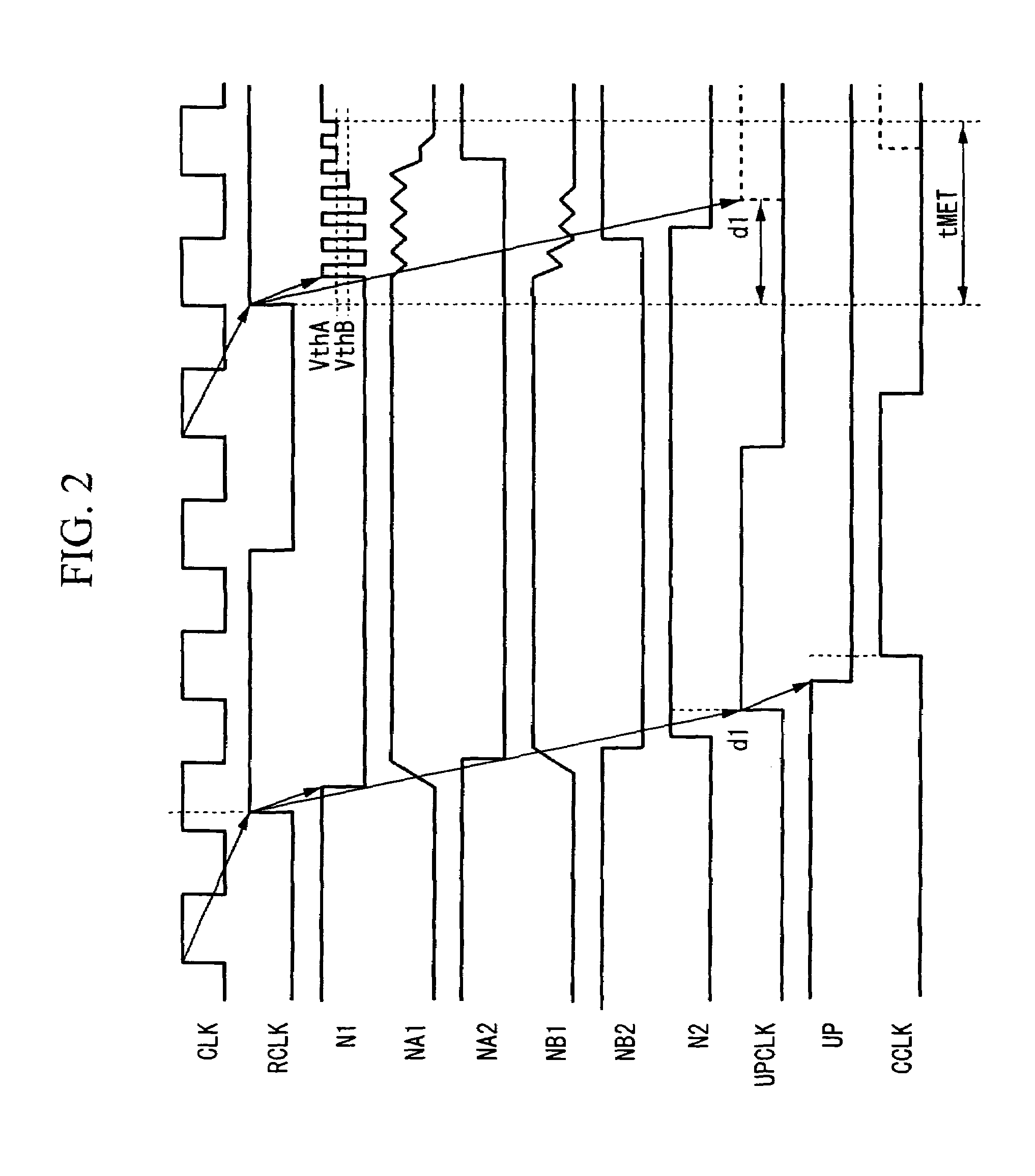
[0039]Reference symbols INVA1 and INVB1 each indicate an inverter used for inverting and outputting the signal output from the inverter 22, wherein the inverter INVA1 has a threshold level VthA which is higher than the threshold level VthB of the inverter INVB1 (see FIG. 2). Such a difference in the threshold ...

second embodiment

[0052]A second embodiment of the present invention will be shown in FIG. 3. In comparison with the first embodiment, the present embodiment has a distinctive feature in which in place of the inverters INVA1 and INVB1 which respectively have the thresholds VthA and VthB, current mirror amplifiers AMPA and AMPB are provided. The reference voltages of the amplifiers AMPA and AMPB are respectively voltages VrefA and VrefB (VrefA>VrefB), which are generated by a resistive division using resistors 41 to 43. The basic operation of the present embodiment is almost identical to that of the first embodiment (refer to FIG. 2). In the present embodiment, logic thresholds can be precisely controlled, and thus be set to optimum values.

[0053]While preferred embodiments of the invention have been described and illustrated above, it should be understood that these are exemplary embodiments of the invention and are not to be considered as limiting. Additions, omissions, substitutions, and other modif...


PUM


Abstract

A phase comparing circuit includes a first storage circuit for reading an external clock signal based on a control clock signal; first and second inverters for inverting a signal from the first storage circuit based respectively on first and second threshold levels; third and fourth inverters for inverting respective signals output from the first and second inverters; a delay circuit for delaying the control clock signal by a specific time; a coincidence control circuit for setting the delayed control clock signal to be active when the signals from the third and fourth inverters coincide with each other, and setting it to be inactive when the signals from the third and fourth inverters do not coincide with each other; and a second storage circuit for reading a signal output form the first storage circuit when the delayed control clock signal is active, and outputting the read signal as the control signal.

Description

BACKGROUND OF THE INVENTION[0001]1. Field of the Invention[0002]The present invention relates to a digital phase comparing circuit, and in particular, relates to a phase comparing circuit for preventing an erroneous operation of a next circuit connected thereto when a metastable phenomenon occurs.[0003]Priority is claimed on Japanese Patent Application No. 2007-059091, filed Mar. 8, 2007, the contents of which are incorporated herein by reference.[0004]2. Description of the Related Art[0005]FIG. 4 is a general circuit diagram of a DLL (delay locked loop) used in a DDR SDRAM (double data rate synchronous dynamic RAM) or the like, and FIG. 5 shows the corresponding operation waveforms.[0006]An external clock (signal) CLK, input into an input circuit 1, is transformed into an output control clock CLK0 via a delay circuit 2 and a buffer 3. Based on the clock CLK0, data DQ and a data control clock DQS are respectively output from a DQ output circuit 4 and a DQS output circuit 5. In this ...

Claims


Application Information

Patent Timeline
Patent Type & Authority Patents(United States)
IPC IPC(8): G01R25/00H03D13/00
CPCH03D13/004
Inventor TAKAI, YASUHIRO
Owner MICRON TECH INC
Why Eureka
Try Eureka