Data holding circuit and signal processing circuit

a signal processing circuit and data holding technology, applied in the direction of pulse generators, pulse techniques, electrical equipment, etc., can solve the problems of generating glitch noise at signal switching timings, difficult to find out at which timing and/or in which signal glitch noise is generated, and reducing current consumption and unnecessary radiation noise, simple structure, and improved process precision

Active Publication Date: 2009-11-24
SHENZHEN TOREY MICROELECTRONIC TECH CO LTD
View PDF4 Cites 1 Cited by
  • Summary
  • Abstract
  • Description
  • Claims
  • Application Information

AI Technical Summary

Benefits of technology

[0010]When signals that are sampled respectively at both a rising edge timing and a falling edge timing of a clock signal are combined, glitch noise is generated due to a variation of delay times of the signals (signals sampled at the rising edge timing and signals sampled at the falling edge timing). Conventionally, a delay circuit, and an OR circuit and / or an AND circuit have been combined, and an OR operation and / or an AND operation with the clock signal and another signal have been performed so as to remove the glitch noise.
[0034]Further, according to a signal processing circuit using the data holding circuit according to the present invention, it is possible to perform a signal process at every half-clock cycle using a clock signal having the same frequency as conventional, thereby improving the precision of the process. In addition, it is possible, by using a clock signal having a frequency that is one-half of a conventional frequency, to perform a signal process at a precision equivalent to the conventional and to reduce a current consumption and unnecessary radiation noise.

Problems solved by technology

However, the conventional technique described above has the following problems.
When signals that are sampled respectively at both a rising edge timing and a falling edge timing of a clock signal are combined, glitch noise is generated due to a variation of delay times of the signals (signals sampled at the rising edge timing and signals sampled at the falling edge timing).
For example, when a conventional signal selection circuit disclosed in Reference 1 selects one signal among an original oscillation clock signal (reference clock signal) and a frequency-divided clock signals obtained by frequency-dividing the original oscillation clock signal, a problem of generating glitch noise at a signal switching timing occurs.
However, it is difficult to find out at which timing and / or in which signal glitch noise is generated.
Still further, when a clock signal is input into a logic circuit, a problem occurs of having the difficulty to set a timing when a layout of the logic circuit is designed.

Method used


Image

  • Data holding circuit and signal processing circuit
  • Data holding circuit and signal processing circuit
  • Data holding circuit and signal processing circuit

Examples


embodiment 1

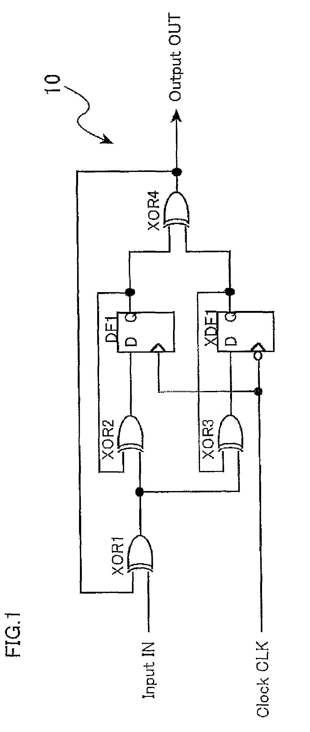
[0050]FIG. 1 is a circuit diagram showing an exemplary essential structure of a data holding circuit 10 according to Embodiment 1 of the present invention.

[0051]In FIG. 1, the data holding circuit 10 according to Embodiment 1 includes: two flip-flops DF1 and XDF1; and four exclusive OR circuits XOR1 to XOR4 for each outputting a signal of ‘0’ (L level) when it receives the same inputs (e.g., L and L, or the like), and outputting a signal of ‘1’ (H level) when it receives different inputs (e.g., H and L, or the like).

[0052]The exclusive OR circuits XOR1 to XOR4 each output a signal of ‘0’ (L level) when it receives the same input signals of ‘0’ or ‘1’, and outputs a signal of ‘1’ (H level) when it receives different input signals of ‘0’ and ‘1’.

[0053]Input ends of the first exclusive OR circuit XOR1 receive an input signal IN and an output signal from the fourth exclusive OR circuit XOR4, respectively. Input ends of the second exclusive OR circuit XOR2 receive an output signal from t...

embodiment 2

[0068]Embodiment 2 will describe a case in which the first flip-flop DF1 and the second flip-flop XDF1 according to Embodiment 1 are each provided with an asynchronous reset terminal R, they are denoted as a first flip-flop DF2 and a second flip-flop XDF2, respectively, and a final output signal OUT can be reset to ‘0’ by a reset signal XR.

[0069]FIG. 3 is a circuit diagram showing an exemplary essential structure of a data holding circuit 20 according to Embodiment 2 of the present invention.

[0070]In FIG. 3, the data holding circuit 20 according to Embodiment 2 includes: first and second flip-flops DF2 and XDF2; and four exclusive OR circuits XOR1 to XOR4.

[0071]An asynchronous reset terminal R is provided to each of the first flip-flop DF2 and the second flip-flop XDF2. The reset terminal R of each of the first flip-flop DF2 and the second flip-flop XDF2 receives a reset signal XR. It should be noted that the other structures in the data holding circuit 20 are similar to those for t...

embodiment 3

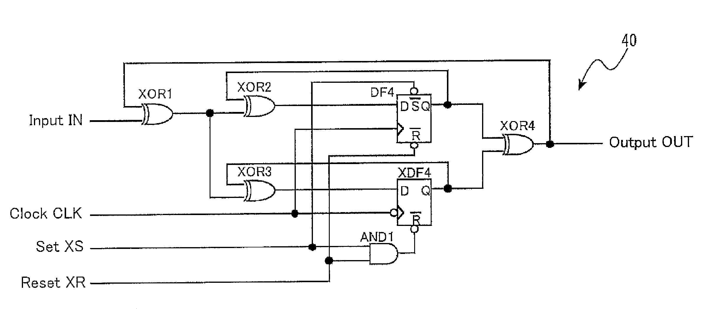
[0078]Embodiment 3 will describe a case in which the first flip-flop DF1 according to Embodiment 1 is provided with an asynchronous set terminal S, and the second flip-flop XDF1 according to Embodiment 1 is provided with an asynchronous reset terminal R, they are denoted as a first flip-flop DF3 and a second flip-flop XDF3, respectively, and a final output signal OUT can be set to ‘1’ by a set signal XS.

[0079]FIG. 5 is a circuit diagram showing an exemplary essential structure of a data holding circuit 30 according to Embodiment 3 of the present invention.

[0080]In FIG. 5, the data holding circuit 30 according to Embodiment 3 includes: first and second flip-flops DF3 and XDF3; and four exclusive OR circuits XOR1 to XOR4.

[0081]The first flip-flop DF3 is provided with an asynchronous set terminal S, and the second flip-flop XDF3 is provided with an asynchronous reset terminal R. A set signal XS is input to each of the set terminal S of the first flip-flop DF3 and the reset terminal R o...


PUM


Abstract

A data holding circuit is capable of latching an input signal at both a rising edge and a falling edge of a clock signal. Several flip-flops and exclusive OR circuits cooperate to achieve this function.

Description

[0001]This Nonprovisional application claims priority under 35 U.S.C. §119(a) on Patent Application 2006-332681 filed in Japan on Dec. 8, 2006, the entire contents of which are hereby incorporated by reference.BACKGROUND OF THE INVENTION[0002]1. Field of the Invention[0003]The present invention relates to: a data holding circuit capable of latching an input signal at both a rising edge timing and a falling edge timing of a clock signal; and a signal processing circuit used in the data holding circuit for communication and for reading data from a variety of disks.[0004]2. Description of the Related Art[0005]Serial communications capable of transmitting and receiving data at a high speed have been recently used when communications are conducted in a wired or wireless manner. For example, USB (Universal Serial Bus) utilized for connection between a computer and a peripheral device thereof, and Serial ATA (Advanced Technology Attachment) for connection with a hard disk or the like are u...

Claims


Application Information

Patent Timeline
Patent Type & Authority Patents(United States)
IPC IPC(8): H03K3/037
CPCH03K3/037H03K3/013
Inventor TANAKA, YUJI
Owner SHENZHEN TOREY MICROELECTRONIC TECH CO LTD
Why Eureka
Try Eureka