Method for electrochemically fabricating three-dimensional structures including pseudo-rasterization of data
a technology of three-dimensional structures and electrochemical fabrication, which is applied in the direction of instruments, originals for photomechanical treatment, nuclear engineering, etc., can solve the problems of destructive separation of masking materials from substrates
- Summary
- Abstract
- Description
- Claims
- Application Information
AI Technical Summary
Benefits of technology
Problems solved by technology
Method used
Image
Examples
first embodiment
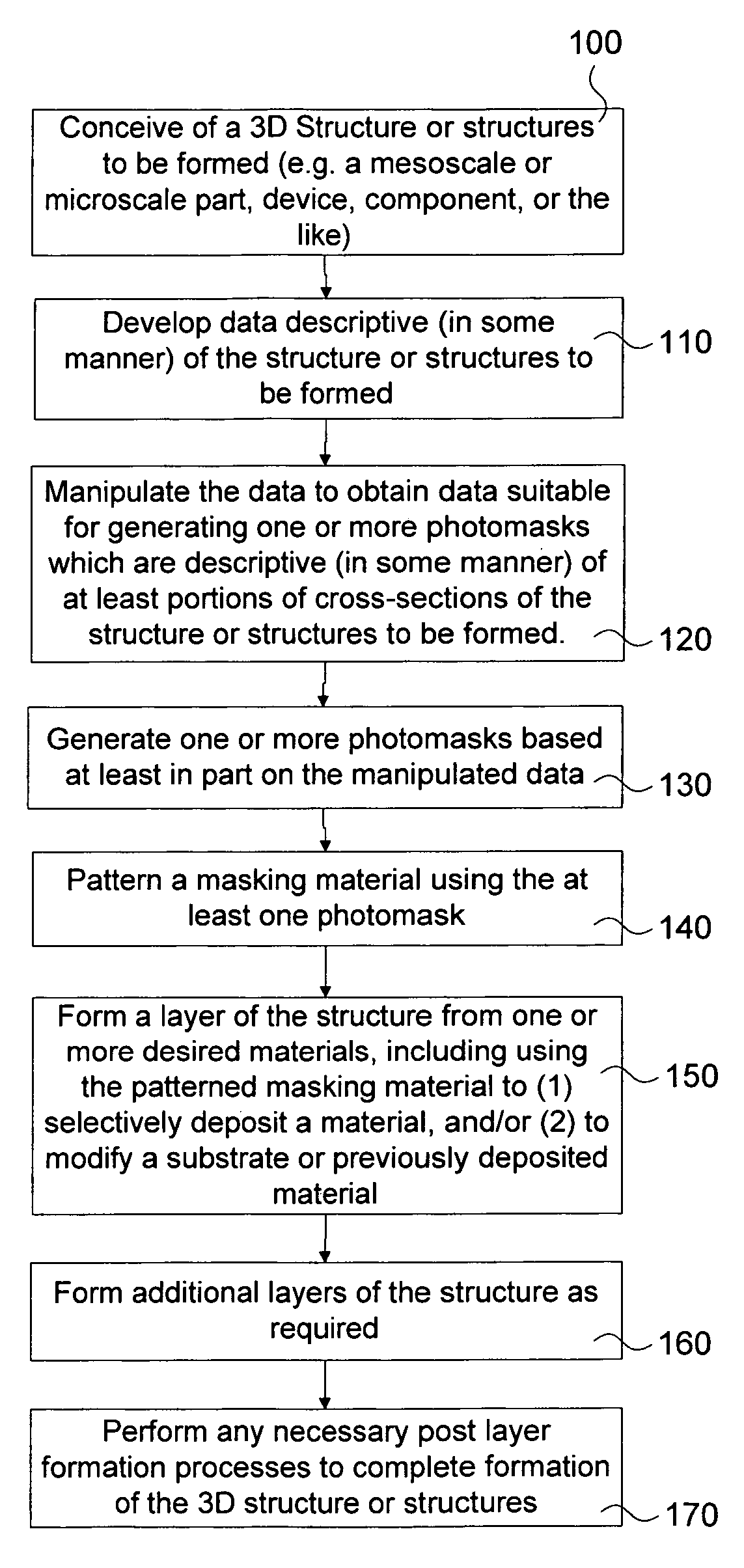
[0062]FIG. 5 provides a block diagram of a process for forming a three-dimensional structure according to the invention including the manipulation of data representing the structure to obtain data suitable for use in creating one or more photomasks that will be used in the fabrication of the structure.
[0063]The block diagram of FIG. 5 begins with block 100 which calls for the conceiving of a three dimensional structure or plurality of structures that one would like to form. The structures may be of any scale; however, the most preferred embodiments of the invention are directed to the formation of mesoscale or microscale structures (e.g. parts, devices, components, or the like).
[0064]Block 110 of the process calls for the development of data that is descriptive of the structure or structures to be formed. This data may take a variety of forms, for example, it may be surface data descriptive of a three dimensional structure, cross sectional data descriptive of one or more layers maki...
second embodiment
[0105]FIG. 15 provides a block diagram of a process for forming a three-dimensional structure according to the invention including the manipulation of data representing the structure to obtain data suitable for use in creating one or more masks that may be used in selectively patterning a substrate or previously deposited material during the fabrication of the structure.
[0106]The process of FIG. 15 is similar to that depicted in FIG. 5 with the exception that the process of FIG. 15 does not produce data that is used to produce a photomask but instead uses the produced data to pattern a masking material that will be directly used in patterning a substrate or depositing a material thereto. The direct patterning of a masking material may occur, for example, by selective scanning of a laser beam over the surface of the masking material wherein different scanning speeds may be used to obtain different levels of exposure or where the intensity of the laser beam striking the surface may be...
PUM
| Property | Measurement | Unit |
|---|---|---|
| Aspect Ratio | aaaaa | aaaaa |
| three-dimensional structure | aaaaa | aaaaa |
| area | aaaaa | aaaaa |
Abstract
Description
Claims
Application Information


