Wafer processing method

a processing method and wafer technology, applied in the direction of basic electric elements, semiconductor/solid-state device manufacturing, electric apparatus, etc., can solve the problems of difficult post-processing handling, reducing quality, and weakness of wafers, so as to improve the bending strength of devices and facilitate the carrying of wafers

Active Publication Date: 2009-12-08
DISCO CORP
View PDF6 Cites 8 Cited by
  • Summary
  • Abstract
  • Description
  • Claims
  • Application Information

AI Technical Summary

Benefits of technology

[0005]It is an object of the present invention to provide a wafer processing method capable of securing the quality of each device even when a wafer is made thin and projecting electrodes embedded in each device from the rear surface of the wafer.
[0018]In the wafer processing method of the present invention, since the wafer is divided into individual devices by carrying out the rear surface grinding step or the rear surface etching step to expose the dividing grooves and the annular groove to the rear surface of the substrate, even when the devices are made thin, the periphery of each device is not chipped unlike when the wafer is cut with a cutting machine. In the wafer processing method of the present invention, since the rear surface etching step comes after the rear surface grinding step, the electrodes can be projected from the rear surface of the substrate and grinding distortion generated on the rear surfaces of the devices by carrying out the rear surface grinding step can be removed, thereby making it possible to improve the bending strength of the devices. Further, in the wafer processing method of the present invention, though the wafer is divided into individual devices in a state where it is affixed to the protective member, the annular reinforcing portion remains and the shape of the wafer is kept, thereby making it possible to carry the wafer easily.

Problems solved by technology

However, since the stiffness of the wafer degrades when the thickness of the wafer is reduced to 100 μm or less, it is difficult to handle it in the post-process.
When such thin wafer is cut along the streets by means of a cutting machine to be divided into individual devices, the periphery of each device is chipped at many positions, thereby reducing its quality.

Method used


Image

  • Wafer processing method
  • Wafer processing method
  • Wafer processing method

Examples


Embodiment Construction

[0030]Preferred embodiments of the present invention will be described in detail hereinunder with reference to the accompanying drawings.

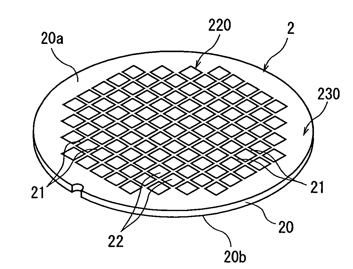
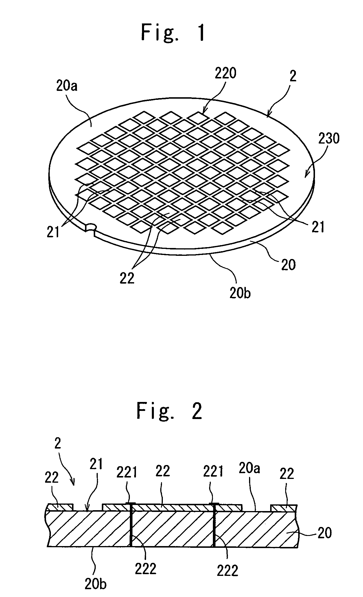
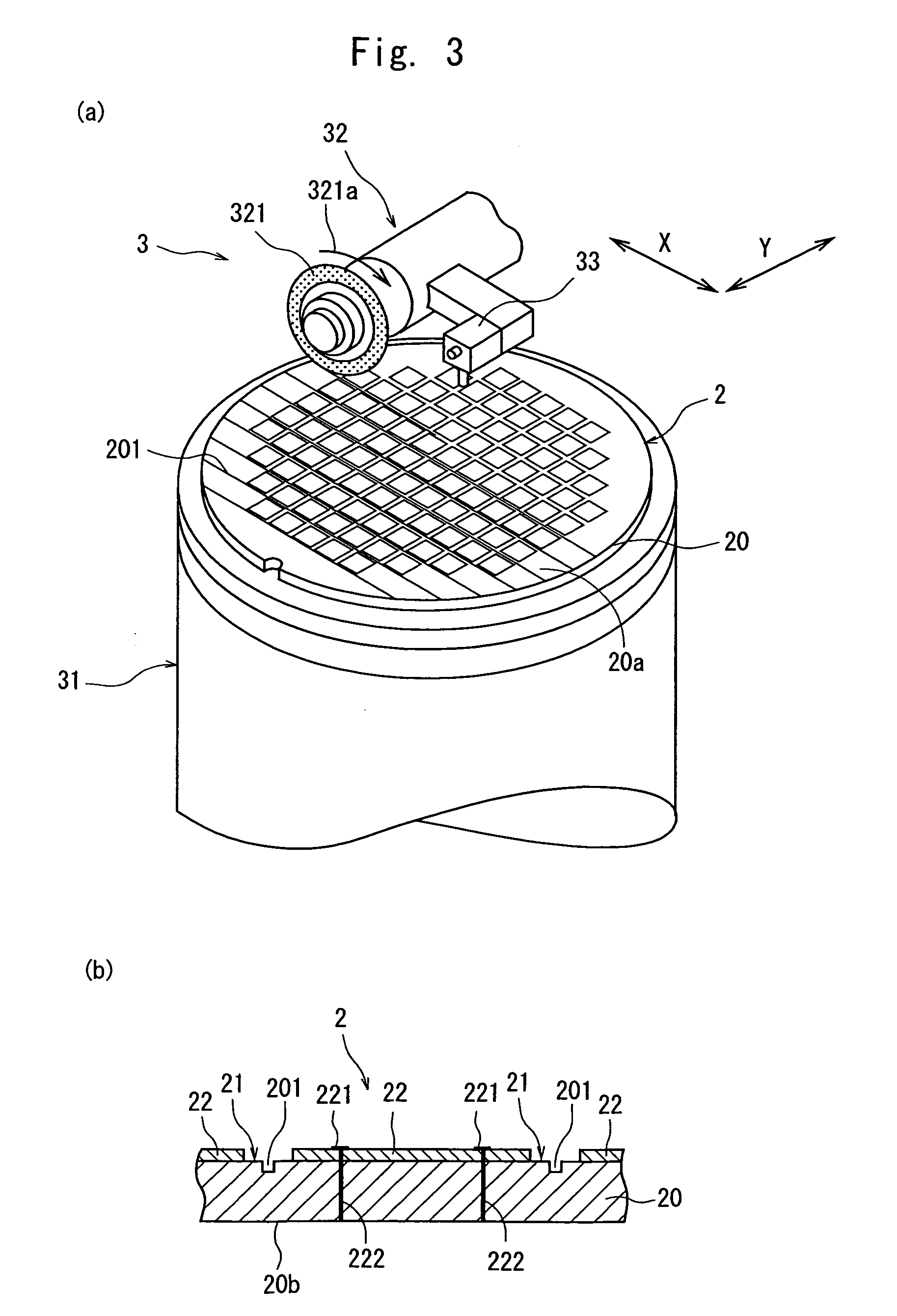
[0031]FIG. 1 is a perspective view of a semiconductor wafer as a wafer to be processed by the wafer processing method of the present invention. The semiconductor wafer 2 shown in FIG. 1 has a plurality of streets 21 which are arranged in a lattice pattern on the front surface 20a of a silicon substrate 20 having a thickness of, for example, 700 μm and devices 22 such as IC's or LSI's which are formed in a plurality of areas sectioned by the plurality of streets 21. This semiconductor wafer 2 has a plurality of bonding pads 221 on the front surface of each device 22 and electrodes 222 which are embedded in the silicon substrate 20 and connected to the respective bonding pads 221. The semiconductor wafer 2 constituted as described above has a device area 220 where the devices 22 are formed and a peripheral extra area 230 surrounding the device area 2...


PUM


Abstract

A wafer processing method for dividing, along streets, a wafer having a device area where devices are formed in a plurality of areas sectioned by the plurality of streets arranged in a lattice pattern on the front surface of a substrate and a peripheral extra area and comprising electrodes which are embedded in the substrate of the device area, comprising a dividing groove forming step for forming dividing grooves having a depth corresponding to the final thickness of each device along the streets; an annular groove forming step for forming an annular groove having a depth corresponding to the final thickness of each device along the boundary between the device area and the peripheral extra area; a protective member affixing step for affixing a protective member to the front surface of the wafer; a rear surface grinding step for grinding a rear surface corresponding to the device area of the substrate of the wafer to expose the dividing grooves and the annular groove to the rear surface of the substrate of the wafer and form an annular reinforcing portion in an area corresponding to the peripheral extra area; and a rear surface etching step for etching the rear surface of the substrate of the wafer to project the electrodes from the rear surface of the substrate.

Description

FIELD OF THE INVENTION[0001]The present invention relates to a method for dividing, along a plurality of streets, a wafer having a device area where devices are formed in a plurality of areas sectioned by the plurality of streets formed in a lattice pattern on the front surface and a peripheral extra area surrounding the device area.DESCRIPTION OF THE PRIOR ART[0002]In the production process of a semiconductor device, a plurality of areas are sectioned by dividing lines called “streets” arranged in a lattice pattern on the front surface of a substantially disk-like semiconductor wafer, and a device such as IC or LSI is formed in each of the sectioned areas. Thus formed semiconductor wafer is generally cut along the streets by using a cutting machine to be divided into individual devices which are widely used in electric equipment.[0003]To downsize electric equipment, a multi-layered laminate type semiconductor device comprising a plurality of devices has been implemented. The method...

Claims


Application Information

Patent Timeline
Patent Type & Authority Patents(United States)
IPC IPC(8): H01L21/00
CPCH01L21/78H01L21/3065
Inventor SEKIYA, KAZUMAKAJIYAMA, KEIICHI
Owner DISCO CORP
Why Eureka
Try Eureka