Thin-film device and method of manufacturing same
a thin film, film technology, applied in the direction of capacitors, semiconductor devices, electrical apparatus, etc., can solve the problems of short-circuit failure, change in capacitance, and reduced withstand voltage of capacitors, so as to suppress capacitor characteristics. , the effect of reducing the variation
- Summary
- Abstract
- Description
- Claims
- Application Information
AI Technical Summary
Benefits of technology
Problems solved by technology
Method used
Image

Examples
first embodiment
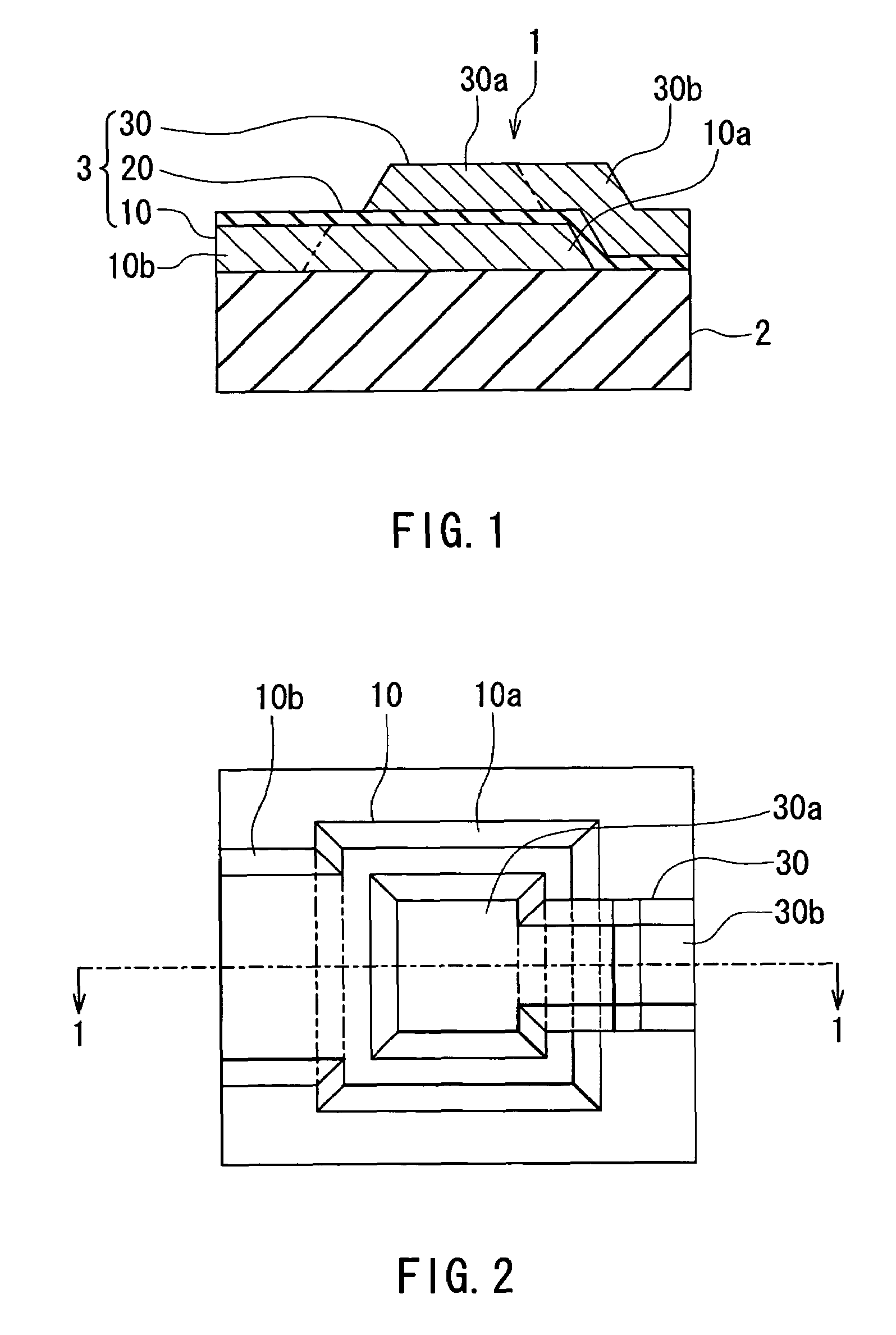
[0049]Reference is now made to FIG. 1 and FIG. 2 to describe a thin-film device of a first embodiment of the invention. FIG. 2 is a top view of the thin-film device of the embodiment. FIG. 1 is a cross-sectional view taken along line 1-1 of FIG. 2. As shown in FIG. 1, the thin-film device 1 of the embodiment comprises a substrate 2 and a capacitor 3 provided on the substrate 2. The capacitor 3 incorporates: a lower conductor layer 10 disposed on the substrate 2; a dielectric film 20 a portion of which is disposed on the lower conductor layer 10; and an upper conductor layer 30 disposed on the dielectric film 20.
[0050]The lower conductor layer 10 incorporates: a lower electrode portion 10a that functions as one of electrodes of the capacitor 3; and a lower transmission line portion 10b that extends from the lower electrode portion 10a to a side thereof and functions as a signal transmission line. The lower conductor layer 10 has a top surface, a side surface, and a corner portion for...
second embodiment
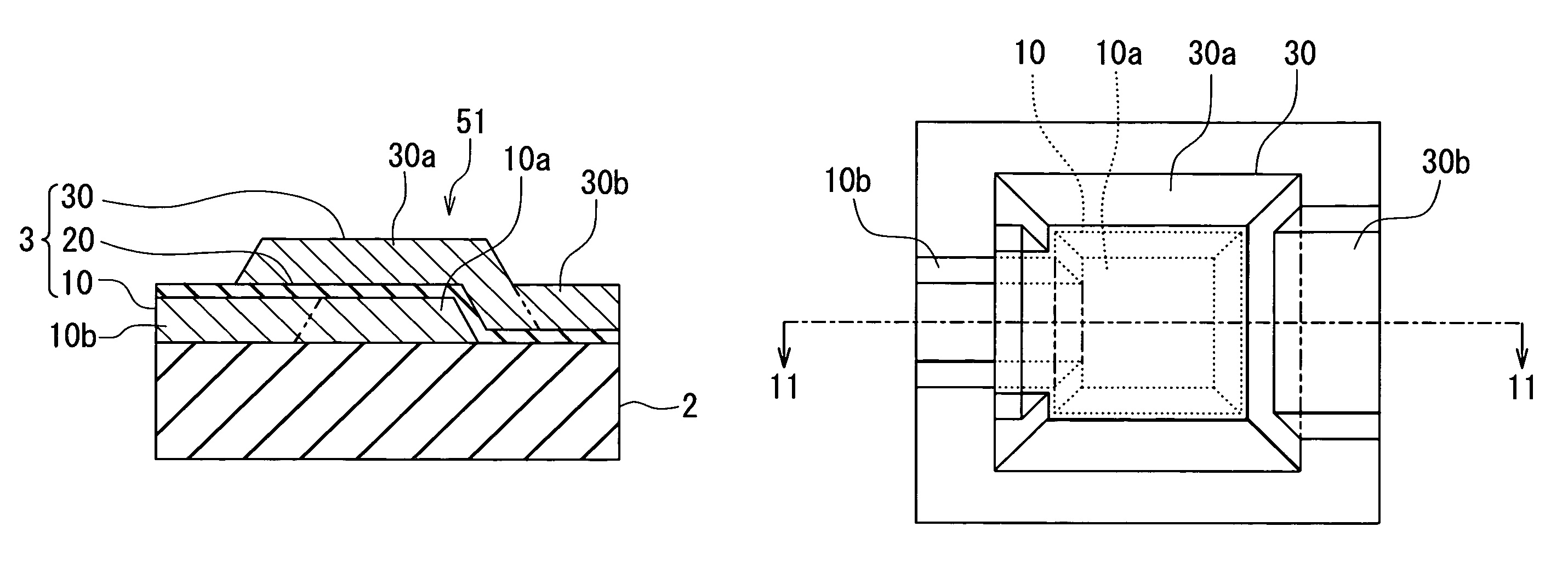
[0078]Reference is now made to FIG. 11 and FIG. 12 to describe a thin-film device of a second embodiment of the invention. FIG. 12 is a top view of the thin-film device of the embodiment. FIG. 11 is a cross-sectional view taken along line 11-11 of FIG. 12. As shown in FIG. 11, the thin-film device 51 of the second embodiment comprises the substrate 2 and the capacitor 3 provided on the substrate 2. The capacitor 3 incorporates: the lower conductor layer 10 disposed on the substrate 2; the dielectric film 20 a portion of which is disposed on the lower conductor layer 10; and the upper conductor layer 30 disposed on the dielectric film 20.
[0079]The lower conductor layer 10 incorporates: the lower electrode portion 10a that functions as one of the electrodes of the capacitor 3; and the lower transmission line portion 10b that extends from the lower electrode portion 10a to a side thereof and functions as a signal transmission line. The lower electrode portion 10a has the top surface, t...
PUM
 Abstract
Description
Claims
Application Information
 - R&D
- Intellectual Property
- Life Sciences
- Materials
- Tech Scout
- Unparalleled Data Quality
- Higher Quality Content
- 60% Fewer Hallucinations
Browse by: Latest US Patents, China's latest patents, Technical Efficacy Thesaurus, Application Domain, Technology Topic, Popular Technical Reports.
© 2025 PatSnap. All rights reserved.Legal|Privacy policy|Modern Slavery Act Transparency Statement|Sitemap|About US| Contact US: help@patsnap.com