Semiconductor integrated circuit having a (BIST) built-in self test circuit for fault diagnosing operation of a memory

a self-testing circuit and integrated circuit technology, applied in the direction of electronic circuit testing, measurement devices, instruments, etc., can solve the problems of difficult to diagnose a fault at the system operating speed of a semiconductor integrated circuit, and the inability to detect detectable fault candidates

Inactive Publication Date: 2010-01-26
KK TOSHIBA
View PDF13 Cites 28 Cited by
  • Summary
  • Abstract
  • Description
  • Claims
  • Application Information

AI Technical Summary

Problems solved by technology

Therefore, the operation is limited by the operating speed of the external tester that is lower than the system operating speed of a semiconductor integrated circuit.
This makes it difficult to diagnose a fault at the system operating speed of a semiconductor integrated circuit.
Consequently, detectable fault candidates cannot be detected only when the fault diagnosis is performed at the system operating speed.

Method used


Image

  • Semiconductor integrated circuit having a (BIST) built-in self test circuit for fault diagnosing operation of a memory
  • Semiconductor integrated circuit having a (BIST) built-in self test circuit for fault diagnosing operation of a memory
  • Semiconductor integrated circuit having a (BIST) built-in self test circuit for fault diagnosing operation of a memory

Examples


first embodiment

(1) First Embodiment

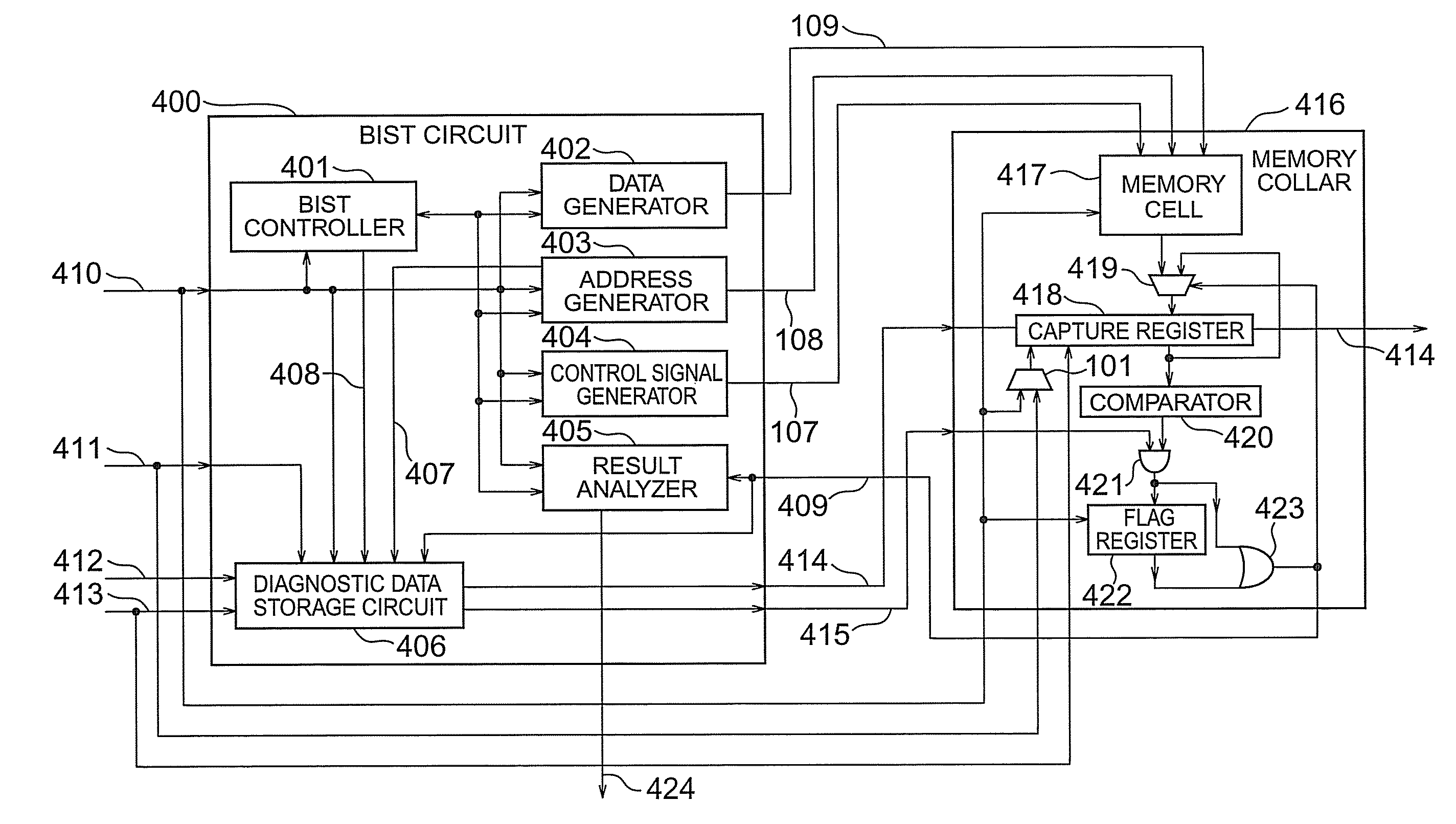
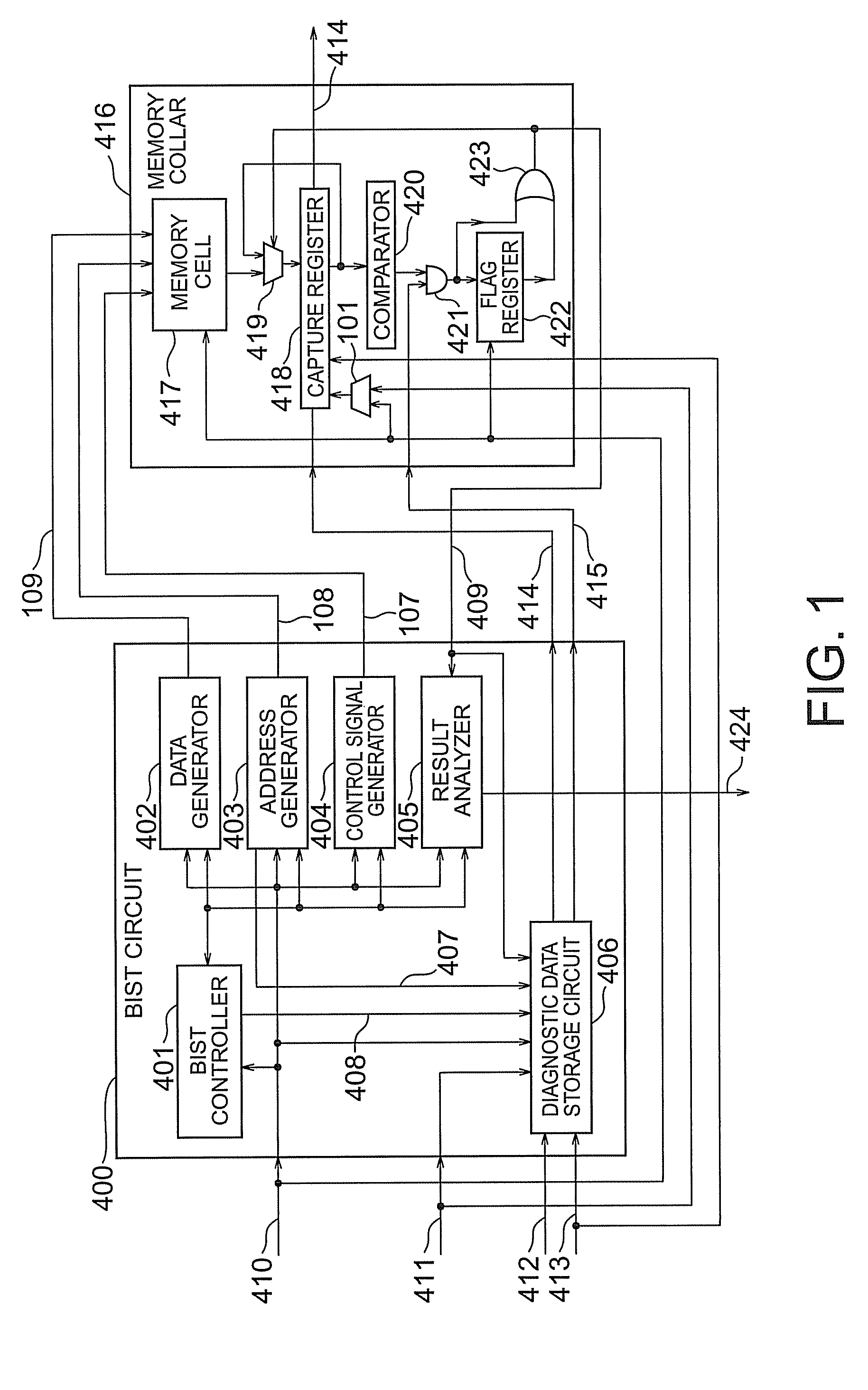
[0068]FIG. 1 shows the arrangement of a semiconductor integrated circuit according to the first embodiment of the present invention.

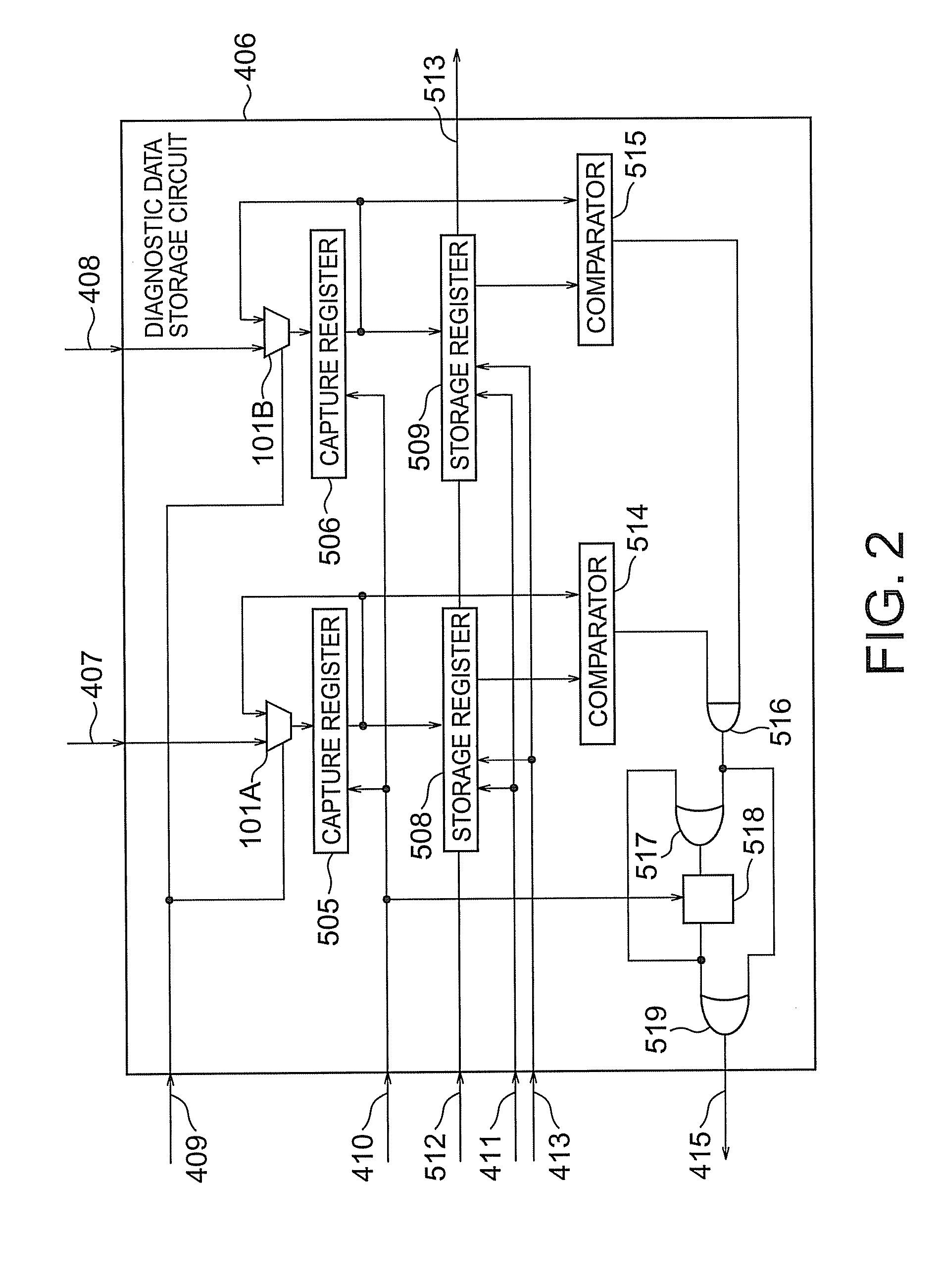
[0069]This semiconductor integrated circuit includes a BIST circuit 400 and memory collar 416. The BIST circuit 400 has a BIST controller 401, data generator 402, address generator 403, control signal generator 404, result analyzer 405, and diagnostic data storage circuit 406. The first embodiment is characterized in that the BIST circuit 400 has the diagnostic data storage circuit 406.

[0070]On the other hand, a block called the memory collar 416 includes a memory cell 417 as an object of a BIST, together with a multiplexer 419, capture register 418, multiplexer 101, comparator 420, AND circuit 421, flag register 422, and OR circuit 423 as elements necessary for a BIST operation.

[0071]In the BIST circuit 400, a high-speed clock 410 is input to the BIST controller 401, data generator 402, address generator 403, control signal generato...

reference example 1

[0157]FIG. 6 shows the arrangement of a semiconductor integrated circuit that performs a BIST operation by using a comparator type memory BIST circuit according to reference example 1.

[0158]A BIST controller 101 in a BIST circuit 100 sequentially generates and outputs control signals necessary to control a data generator 102, address generator 103, and control signal generator 104.

[0159]A block called a memory collar 111 contains a memory 112 as an object of the BIST, in addition to a capture register 113, comparator 114, and flag register 115 as logic elements necessary for the BIST operation.

[0160]The memory 112 receives write data 109 and an expected value 110 generated by the data generator 102, address data 108 generated by the address generator 103, and a control signal 107 generated by the control signal generator 104.

[0161]The capture register 113 receives the output from the memory 112. The comparator 114 compares the output from the capture register 113 with the data expec...

reference example 2

[0164]FIG. 7 shows the arrangement of a semiconductor integrated circuit that performs a BIST by using a compaction type memory BIST circuit according to reference example 2.

[0165]A BIST controller 201 in a BIST circuit 200 sequentially generates and outputs control signals necessary to control a data generator 202, address generator 203, control signal generator 204, and result analyzer 205. A memory collar 210 includes a memory 211 as an object of the BIST, in addition to a compactor 212.

[0166]The memory 211 receives write data 209 generated by the data generator 202, address data 208 generated by the address generator 203, and a control signal 207 generated by the control signal generator 204. The compactor 212 receives the output from the memory 211, and sequentially compresses and outputs the data.

[0167]The result analyzer 205 compares the value saved in the compactor 212 at the end of the BIST with an expected value to check the result of the BIST, and outputs the result as a ...


PUM


Abstract

According to the present invention, there is provided a semiconductor integrated circuit having: a BIST including a data generator, an address generator, a control signal generator, a result analyzer, a BIST controller, and a diagnostic data storage circuit including a first capture register which captures and outputs, in accordance with a first clock, a latest address signal and the BIST state signal output from said BIST controller while the flag signal is in as state that no fault is detected, and maintains outputs when the flag signal is in a state that a fault is detected. The semiconductor integrated circuit can further include a memory collar having a memory cell, a second capture register, a comparator, and a flag register. The semiconductor integrated circuit can perform a fault diagnosing operation of a memory by using a comparator type BIST circuit.

Description

CROSS REFERENCE TO RELATED APPLICATION[0001]This application is based upon and claims benefit of priority under 35 USC §119 from the Japanese Patent Application No. 2006-188391, filed on Jul. 7, 2006, the entire contents of which are incorporated herein by reference.BACKGROUND OF THE INVENTION[0002]The present invention relates to a semiconductor integrated circuit and, more particularly, to a semiconductor integrated circuit that incorporates a built-in self test circuit of a memory and performs a fault diagnosing operation by using this circuit.[0003]There is a method that detects a defective chip by performing a built-in self test (to be referred to as a BIST hereinafter) by using a BIST circuit incorporated into a semiconductor integrated circuit including a memory, and diagnoses faults in the defective chip by using the BIST circuit, thereby extracting candidates of defective portions of the memory.[0004]Examples of the BIST circuit are a comparator type BIST circuit and compac...

Claims


Application Information

Patent Timeline
Patent Type & Authority Patents(United States)
IPC IPC(8): G01R31/28
CPCG11C29/16G11C29/38G11C29/44G11C2029/0405G11C2029/2602G11C2029/3602
Inventor ANZOU, KENICHITOKUNAGA, CHIKAKO
Owner KK TOSHIBA
Why Eureka
Try Eureka