Protective circuit board for battery pack

a protection circuit board and battery pack technology, applied in the direction of circuit electrostatic discharge protection, secondary cell servicing/maintenance, printed circuit non-printed electric components association, etc., can solve the problems of conventional battery pack frequently malfunctioning, noise or static, and the protection circuit board of the battery pack is often exposed to extreme conditions, so as to reduce noise and minimize influence

Active Publication Date: 2010-02-23
SAMSUNG SDI CO LTD
View PDF11 Cites 6 Cited by
  • Summary
  • Abstract
  • Description
  • Claims
  • Application Information

AI Technical Summary

Benefits of technology

[0011]Accordingly, a protective circuit board for a battery pack is provided with main signal patterns disposed inside an insulation layer to minimize the influence of external electromagnetic waves and static electricity.
[0014]Since main signal patterns are positioned inside the insulation layer, external electromagnetic waves and static electricity are less likely to reach the signal patterns. Therefore, various electronic components mounted on the protective circuit board are not affected by any noise caused by electromagnetic waves and static electricity, and the protective circuit board may be less likely to malfunction.
[0015]In addition, the first and second dummy patterns, which are positioned above and below the signal pattern, respectively, absorb and remove electromagnetic waves and static electricity. As a result, the signal pattern, which is positioned between the dummy patterns, is less affected by noise.
[0016]A method of minimizing influence of electromagnetic waves and static electricity on signal patterns of a protective circuit board for a battery pack includes providing the protective circuit board with an insulation layer. The insulation layer has a first outer surface, a second outer surface, and a first insulation sublayer and a second insulation sublayer interposed between the first outer surface and the second outer surface. The method also includes disposing a first signal pattern at a first interface between the first insulation sublayer and the second insulation sublayer such that the first signal pattern is spaced from the first outer surface and the second outer surface.

Problems solved by technology

Battery packs having a protective circuit board mounted thereon are frequently exposed to extreme conditions.
Particularly, noise or static electricity may act on the electronic components along first or second signal patterns formed on the surface of the protective circuit board.
As a result, conventional battery packs frequently malfunction as various electronic components fail to operate correctly under the influence of electromagnetic waves or static electricity.
However, such measures raise the overall manufacturing cost of battery packs and increase the weight.

Method used


Image

  • Protective circuit board for battery pack
  • Protective circuit board for battery pack
  • Protective circuit board for battery pack

Examples


Embodiment Construction

[0021]Hereinafter, examples of embodiments of the present invention will be described with reference to the accompanying drawings. In the following description and drawings, the same reference numerals are used to designate the same or similar components, and repetition of the description on the same or similar components will be omitted.

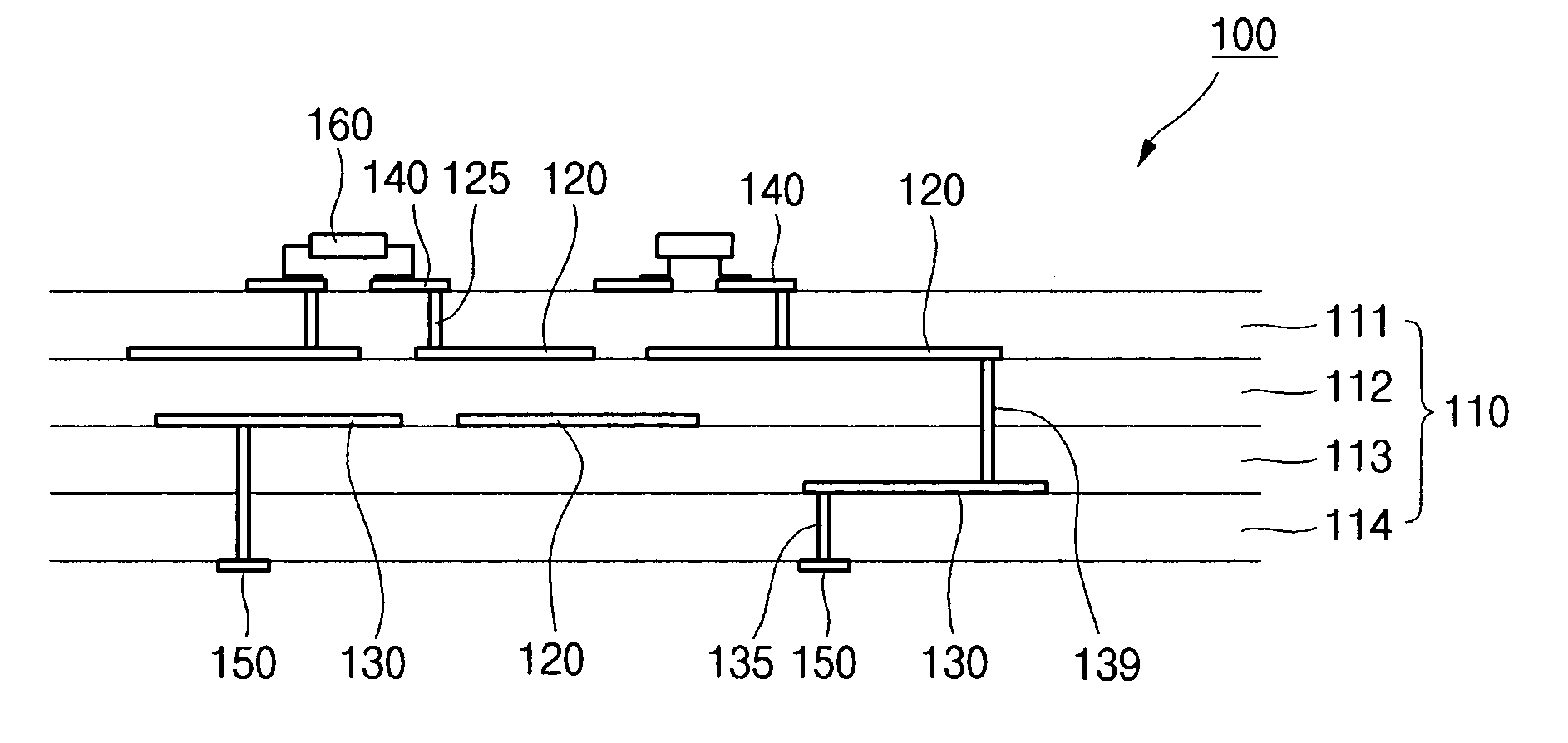
[0022]As shown in FIG. 2, a protective circuit board 100 for a battery pack according to one embodiment of the present invention includes at least one insulation layer 110, at least one first signal pattern 120 disposed inside insulation layer 110, at least one second signal pattern 130 disposed inside the insulation layer 110, a first signal pad 140 formed on a surface of the insulation layer 110 while being electrically connected to the first signal pattern 120, and a second signal pad 150 formed on a surface of the insulation layer 110 while being electrically connected to the second signal pattern 130.

[0023]The insulation layer 110 in FIG. 2 has...


PUM


Abstract

A protective circuit board for a battery pack for controlling charge and discharge states of the battery pack includes an insulation layer and a first signal pattern disposed inside the insulation layer. The circuit can further include a second signal pattern disposed inside the insulation layer. The circuit can include a first dummy pattern spaced from a first side of the first signal pattern and a second dummy pattern spaced from a second side of the first signal pattern.

Description

CROSS-REFERENCE TO RELATED APPLICATION[0001]This application claims priority to and the benefit of Korean Patent Application No. 10-2004-0086896, filed with the Korean Intellectual Property Office on Oct. 28, 2004, the entire content of which is incorporated by reference.BACKGROUND OF THE INVENTION[0002]a. Technical Field[0003]The present invention relates to a protective circuit board for a battery pack, and more particularly to a protective circuit board for a battery which minimizes the influence of external electromagnetic waves and static electricity.[0004]b. Description of Related Art[0005]In general, a protective circuit board for a battery pack controls charge and discharge states of the battery pack and interrupts the current of the battery pack when it is overcharged or over-discharged to protect the battery pack and the user.[0006]The structure of a protective circuit board will now be described briefly with reference to FIG. 1.[0007]As shown, a conventional protective ci...

Claims


Application Information

Patent Timeline
Patent Type & Authority Patents(United States)
IPC IPC(8): H05K7/00
CPCH01M10/425H01M10/48H05K1/0259H05K2201/09781H05K1/113H05K2201/09436H05K1/0298Y02E60/10H01M10/46H01M10/44
Inventor YUN, CHANG YONG
Owner SAMSUNG SDI CO LTD
Why Eureka
Try Eureka