Logic circuit for use in a latch circuit and a data reading circuit or the like which includes such a latch circuit

a logic circuit and latch circuit technology, applied in logic circuits, pulse generators, pulse techniques, etc., can solve the problems of output data error, high and low data signal levels are not determined properly, and output waveform suffers synchronization distortion with the clock signal, so as to improve the suppressing error rate and prevent the effect of synchronization distortion

Inactive Publication Date: 2010-03-02
NEC CORP
View PDF8 Cites 0 Cited by
  • Summary
  • Abstract
  • Description
  • Claims
  • Application Information

AI Technical Summary

Benefits of technology

[0018]The present invention has been made in order to solve the problems of the conventional art described above. It is an object of the present invention to provide a high-speed logic circuit for suppressing a waveform distortion due to a clock signal interference and improving an error rate.
[0020]Since the potential stabilizing circuit is connected between the first differential transistor pair and the first transistor, when the first transistor operates in response to the clock signal to supply a current to the common emitter of the first differential transistor pair, a distortion in synchronism with the clock signal is prevented from occurring at the common emitter.
[0021]The logic circuit according to the present invention stabilizes the potential at the common emitter of the differential transistor pair which processes the data signal. Thus, there is provided a high-speed logic circuit with an improved error rate for suppressing a distortion (clock signal interference) of the output waveform which is produced in synchronism with the clock signal.

Problems solved by technology

When there is a large variation in synchronism with the clock signal, it is considered that the variation is superposed as noise on an input potential applied to a differential pair, causing the output waveform to suffer a distortion in synchronism with the clock signal.
If the clock signal interference increases, high and low levels of the data signal are not determined properly, and an error tends to be produced in the output data.

Method used


Image

  • Logic circuit for use in a latch circuit and a data reading circuit or the like which includes such a latch circuit
  • Logic circuit for use in a latch circuit and a data reading circuit or the like which includes such a latch circuit
  • Logic circuit for use in a latch circuit and a data reading circuit or the like which includes such a latch circuit

Examples


1st embodiment

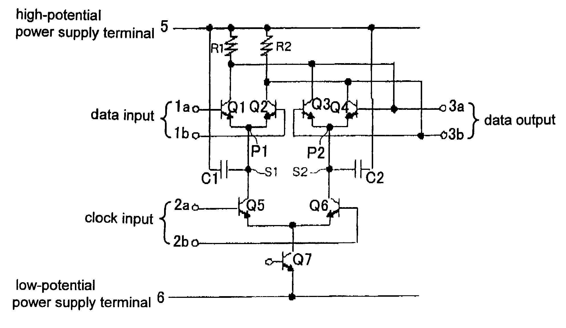
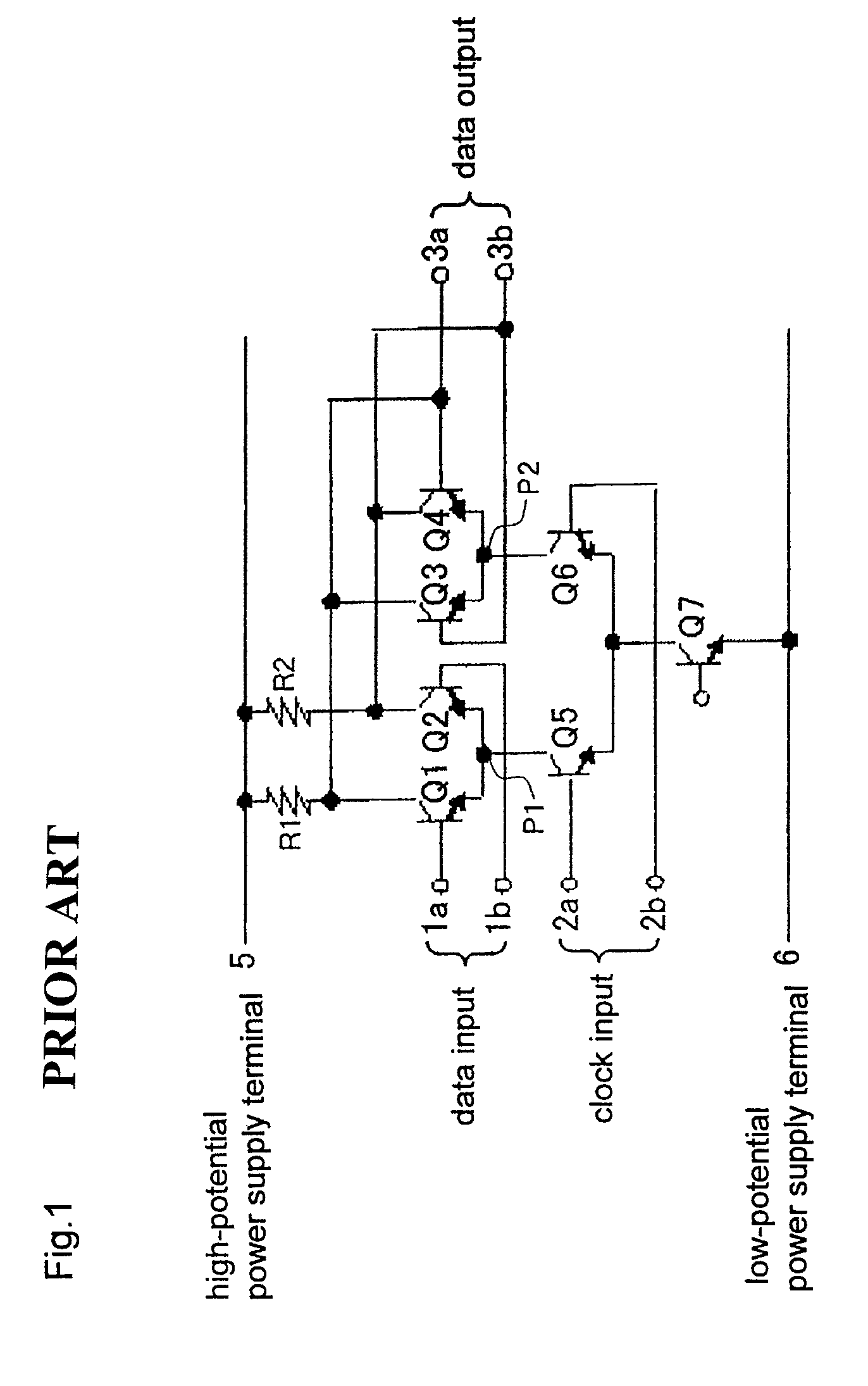
[0055]An arrangement of a latch circuit according to the present embodiment will be described below. FIG. 5 is a circuit diagram of the latch circuit according to the present embodiment. Those parts of the latch circuit which are identical to those of the latch circuit shown in FIG. 1 are denoted by identical reference characters, and will not be described in detail below.

[0056]As shown in FIG. 5, the latch circuit according to the present embodiment has potential stabilizing circuits 30a, 30b connected respectively to junction S1 between common emitter point P1 of the first differential pair and the third differential pair and junction S2 between common emitter point P2 of the second differential pair and the third differential pair in the arrangement shown in FIG. 1.

[0057]For solving the problems, attention is paid to the potentials at the common emitter points of the differential pairs of the data signal processor as a cause of a clock signal interference. Since each of common em...

2nd embodiment

[0067]A latch circuit according to the present embodiment employs capacitors as potential stabilizing circuits. The latch circuit according to the present embodiment will be described below. FIG. 8 is a diagram showing an arrangement of the latch circuit according to the present embodiment. Those parts of the latch circuit which are identical to those of the latch circuit shown in FIG. 5 are denoted by identical reference characters, and will not be described in detail below.

[0068]In FIG. 8, capacitor C1 is connected between high-potential power supply terminal 5 and junction S1 and capacitor C2 is connected between high-potential power supply terminal 5 and junction S2, as the potential stabilizing circuits shown in FIG. 5.

[0069]A master-slave flip-flop circuit employing the latch circuit shown in FIG. 8 will be described below. FIG. 9 is a diagram showing an example of a flip-flop circuit employing the latch circuit shown in FIG. 8. Those parts of the flip-flop circuit which are i...

3rd embodiment

[0084]A latch circuit according to the present embodiment employs resistance dividing circuits as potential stabilizing circuits. The latch circuit according to the present embodiment will be described below. FIG. 14 is a diagram showing an arrangement of the latch circuit according to the present embodiment. Those parts of the latch circuit which are identical to those of the latch circuit shown in FIG. 5 are denoted by identical reference characters, and will not be described in detail below.

[0085]The latch circuit shown in FIG. 14 has resistance dividing circuits as the potential stabilizing circuits shown in FIG. 5. Junction S1 between common emitter point P1 of the first differential pair and the third differential pair is connected to high-potential power supply terminal 5 through resistor R11 and also to low-potential power supply terminal 6 through resistor R12. Junction S2 between common emitter point P2 of the second differential pair and the third differential pair is con...


PUM


Abstract

A logic circuit is provided with a first differential transistor pair (Q1, Q2) operable in response to a data signal input thereto; a current source for supplying a current to the first differential transistor pair (Q1, Q2); a first transistor (Q5) connected between a common emitter of the first differential transistor pair (Q1, Q2) and the current source, and operable in response to a clock signal input thereto; and a first potential stabilizing circuit (30a) connected to a first junction between the common emitter of the first differential transistor pair (Q1, Q2) and a collector of the first transistor (Q5), for stabilizing a potential at said first junction.

Description

[0001]This application claims priority from PCT Application No. PCT / JP2005 / 018342 filed Oct. 4, 2005, and from Japanese Patent Application No. 2004-292678 filed Oct. 5, 2004, which applications are incorporated herein by reference.TECHNICAL FIELD[0002]The present invention relates to a logic circuit for use in a latch circuit and a data reading circuit or the like which includes such a latch circuit.BACKGROUND ART[0003]Latch circuits are used as basic component circuits of logic circuits in many semiconductor integrated circuits. An arrangement of a conventional latch circuit will be described below.[0004]FIG. 1 is a diagram showing an arrangement of a conventional latch circuit. The latch circuit shown in FIG. 1 is used in applications which require high-speed operation. In the description which follows, bipolar transistors are used as active devices.[0005]As shown in FIG. 1, the latch circuit generally employs a differential logic circuit comprising differential transistor pairs (...

Claims


Application Information

Patent Timeline
Patent Type & Authority Patents(United States)
IPC IPC(8): H03K3/00
CPCH03K3/2885
Inventor AMAMIYA, YASUSHI
Owner NEC CORP
Why Eureka
Try Eureka