Pixel circuit and light emitting display using the same

a technology of light-emitting display and pixel circuit, which is applied in the direction of electroluminescent light sources, static indicating devices, instruments, etc., can solve the problems of requiring a longer a substantial amount of time to charge the data line, and insufficient time to charge the load of the data line. , to achieve the effect of increasing the current amount of the data signal, reducing the current write time, and low luminance valu

Active Publication Date: 2010-03-16
SAMSUNG DISPLAY CO LTD
View PDF24 Cites 17 Cited by
  • Summary
  • Abstract
  • Description
  • Claims
  • Application Information

AI Technical Summary

Benefits of technology

[0020]Accordingly, it is an aspect of the present invention to provide a light emitting display, which reduces a current write time while having a low luminance value by increasing a current amount of a data signal. Other aspects of the present invention reduce the number of elements, increase the aperture ratio, and minimize color separation in the light emitting display by connecting a plurality of light emitting diodes to each pixel circuit.

Problems solved by technology

However, the current programming type pixel circuit mentioned above has a problem in that it takes a substantial amount of time to charge the data line since it should control a very small current.
Since a line time is only several tens of microseconds, there is not sufficient time to charge this load to the data line.
In particular, when a low luminance is displayed, since a current value is small, a longer time is required to charge the load of the data line.
Moreover, because one light emitting control line is coupled to each pixel row, the aperture ratio of a light emitting display may be deteriorated.

Method used


Image

  • Pixel circuit and light emitting display using the same
  • Pixel circuit and light emitting display using the same
  • Pixel circuit and light emitting display using the same

Examples


first embodiment

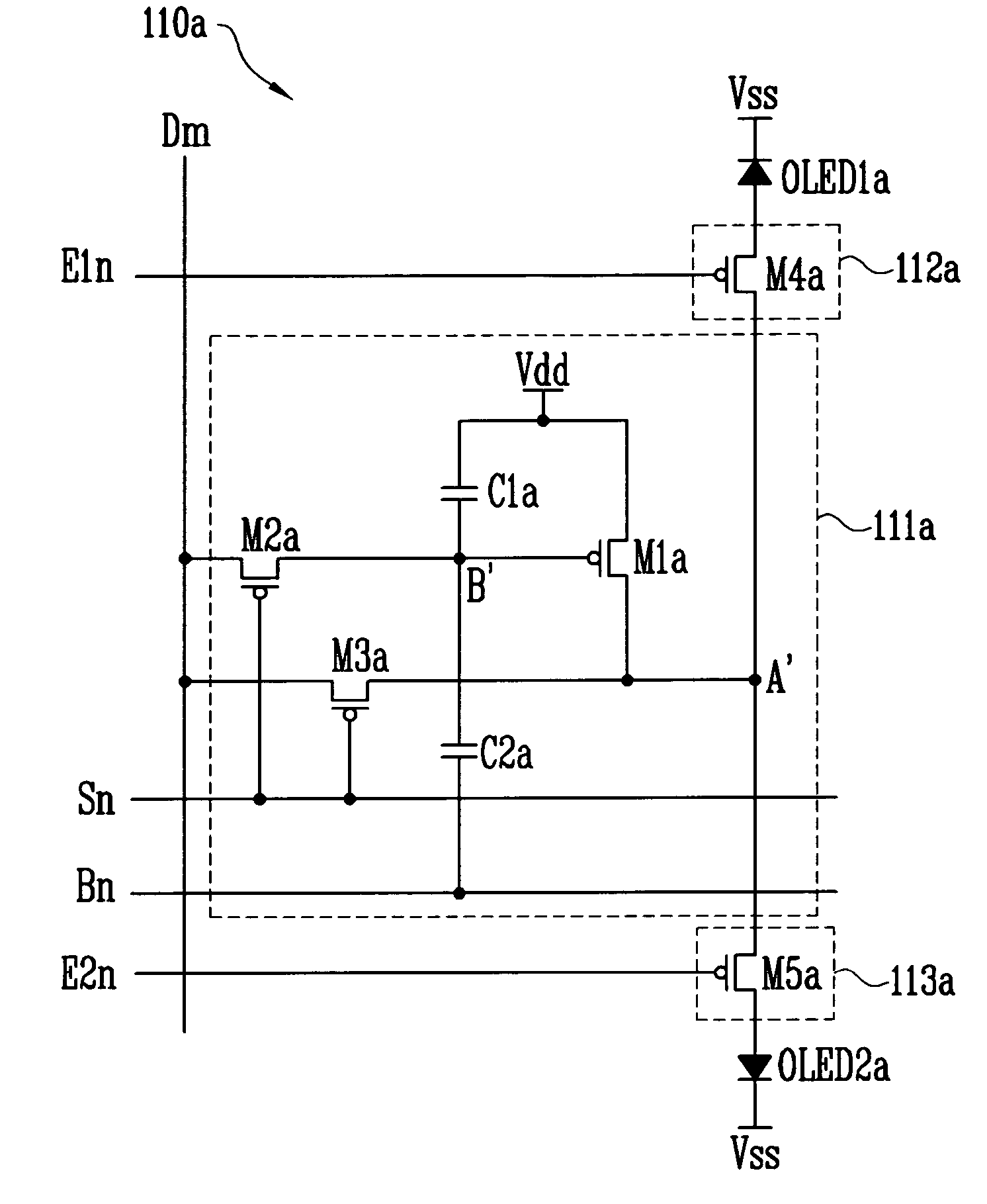
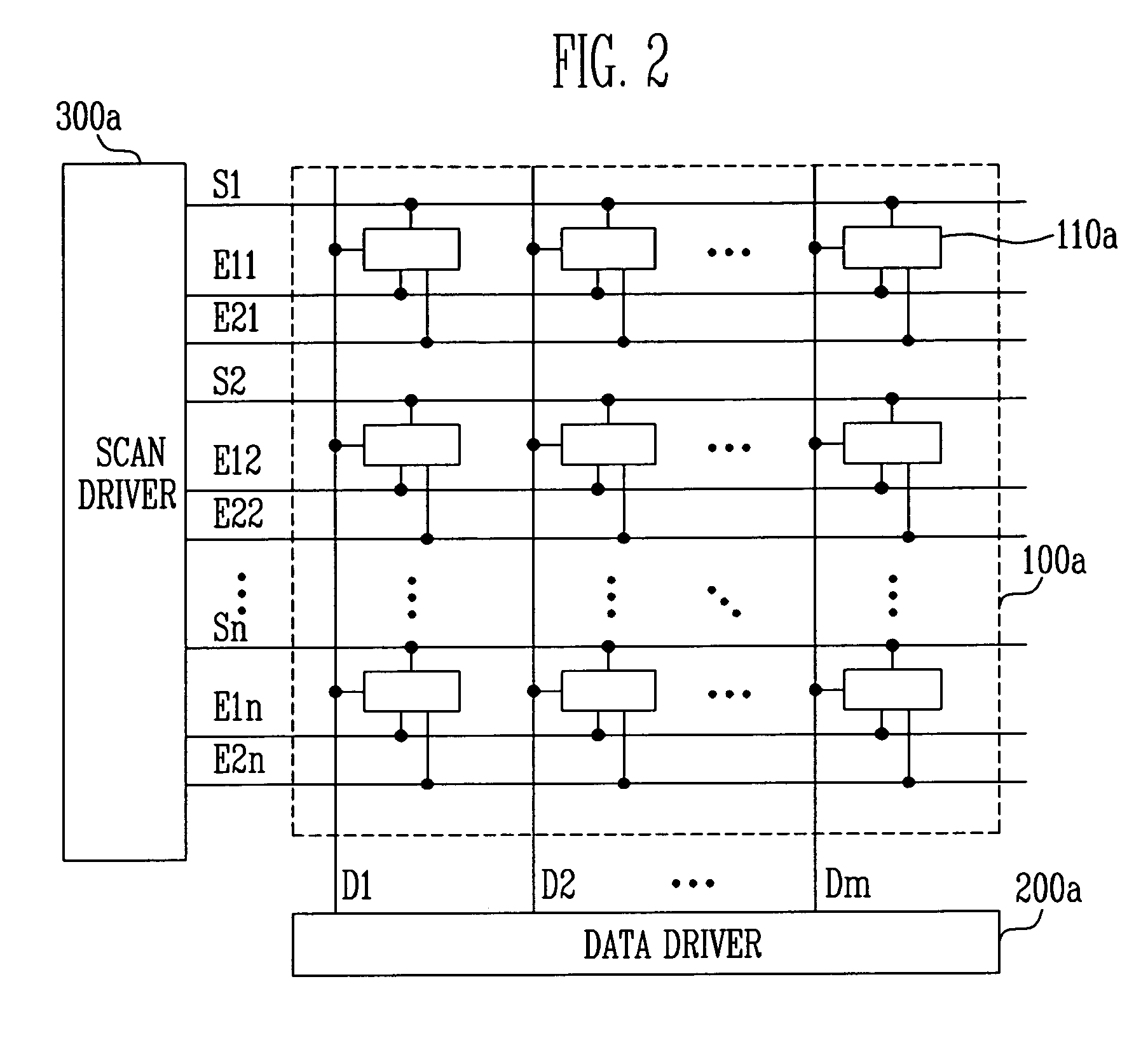
[0034]FIG. 2 is a schematic view showing a structure of a light emitting display according to the present invention. With reference to FIG. 2, the light emitting display includes an image display device 100a, a data driver 200a, and a scan driver 300a.

[0035]The image display device 100a includes a plurality of pixels 110a, a plurality of scan lines S1, S2, S3, . . . Sn-1, Sn, a plurality of first light emitting control lines E11, E12, . . . E1n-1, E1n and a plurality of second light emitting control lines E21, E22, . . . E2n-1, E2n all arranged in a column direction. The device also includes a plurality of data lines D1, D2, . . . Dm-1, Dm arranged in a row direction, and a plurality of pixel power lines (not shown) for supplying power to the pixels. Each of the power lines receives external power and supplies it to the pixels.

[0036]When a data signal is transferred to a pixel 110a through the data lines D1, D2, . . . Dm-1, Dm according to a scan signal on the scan lines S1, S2, S3...

second embodiment

[0039]FIG. 3 is a schematic view showing a structure of a light emitting display according to the present invention. Referring to FIG. 3, the light emitting display includes an image display device 100b, a data driver 200b, and a scan driver 300b.

[0040]The image display device 100b includes a plurality of pixels 110b, a plurality of scan lines S0, S1, S2, . . . Sn-1, Sn, a plurality of first light emitting control lines E11, E12, . . . E1n-1, E1n, a plurality of second light emitting control lines E21, E22, . . . E2n-1, E2n, and a plurality of third light emitting control lines E31, E32, . . . E3n-1, E3n all arranged in a column direction. The device also includes a plurality of data lines D1, D2, . . . Dm-1, Dm arranged in a row direction, and a plurality of pixel power lines (not shown) for supplying power to the pixels. Each of the power lines receives external power and supplies it to the pixels.

[0041]When a data signal is transferred to a pixel 110b through the data lines D1, ...


PUM


Abstract

A light emitting display includes a plurality of light emitting diodes within a pixel. A drive circuit is coupled to the plurality of light emitting diodes and generates a drive current flowing through the light emitting diodes corresponding to a data current. A switch circuit assembly is coupled to the plurality of light emitting diodes and the drive circuit and sequentially transfers the drive current from the drive circuit to the plurality of light emitting diodes. The light emitting diodes sequentially emit light. When all the light emitting diodes emit light, one frame is formed.

Description

CROSS-REFERENCE TO RELATED APPLICATIONS[0001]This application claims priority to and the benefit of Korean Patent Application No. 10-2004-95978, filed on Nov. 22, 2004, in the Korean Intellectual Property Office, the entire disclosure of which is incorporated herein by reference.BACKGROUND[0002]a) Field of the Invention[0003]The present invention relates to a pixel circuit and a light emitting display, and more particularly, to a pixel circuit and a light emitting display using the same, which emits light by a plurality of light emitting diodes coupled to one pixel circuit in order to improve the aperture ratio of the light emitting display.[0004]b) Discussion of Related Art[0005]In recent years, various display devices having reduced weight and volume compared to those of a cathode ray tube have been developed. In particular, light emitting displays having excellent light-emission, a wide angle of visibility, and a high-speed response have been proposed as next-generation planar ty...

Claims


Application Information

Patent Timeline
Patent Type & Authority Patents(United States)
IPC IPC(8): G09G3/32G09G3/20G09G3/30H01L51/50H05B33/14H05B44/00
CPCG09G3/325G09G2300/0465G09G2300/0804G09G2300/0819G09G2300/0852G09G2310/0251G09G2320/0252G09G2320/0242G09G3/30
Inventor KWAK, WON KYU
Owner SAMSUNG DISPLAY CO LTD
Why Eureka
Try Eureka