Digital clock filter circuit for a gapped clock of a non-isochronous data signal having a selected one of at least two nominal data rates

a digital clock and data signal technology, applied in the field of telecommunications, can solve problems such as becoming very complex, and achieve the effects of less circuit board area, reduced power consumption, and reduced component cos

Inactive Publication Date: 2010-04-20
ALCATEL LUCENT SAS
View PDF6 Cites 5 Cited by
  • Summary
  • Abstract
  • Description
  • Claims
  • Application Information

AI Technical Summary

Benefits of technology

[0009]The clock filter circuit according to the invention requires less circuit board area, lower component costs and shows a lower power consumption than existing solutions. It allows full integration into AISCs and provides a simple configuration of the clock rate by simply adapting the PLL algorithm (i.e., the rules according to which the switching is performed). Moreover, it is less prone to crosstalk from neighboring channels, which in existing solutions could cause a false lock problem.

Problems solved by technology

For such applications, the bit rates must be accommodated to the actually used signal type, which might become very complex for narrow band PLLs at the outputs a network element.

Method used


Image

  • Digital clock filter circuit for a gapped clock of a non-isochronous data signal having a selected one of at least two nominal data rates
  • Digital clock filter circuit for a gapped clock of a non-isochronous data signal having a selected one of at least two nominal data rates
  • Digital clock filter circuit for a gapped clock of a non-isochronous data signal having a selected one of at least two nominal data rates

Examples


Embodiment Construction

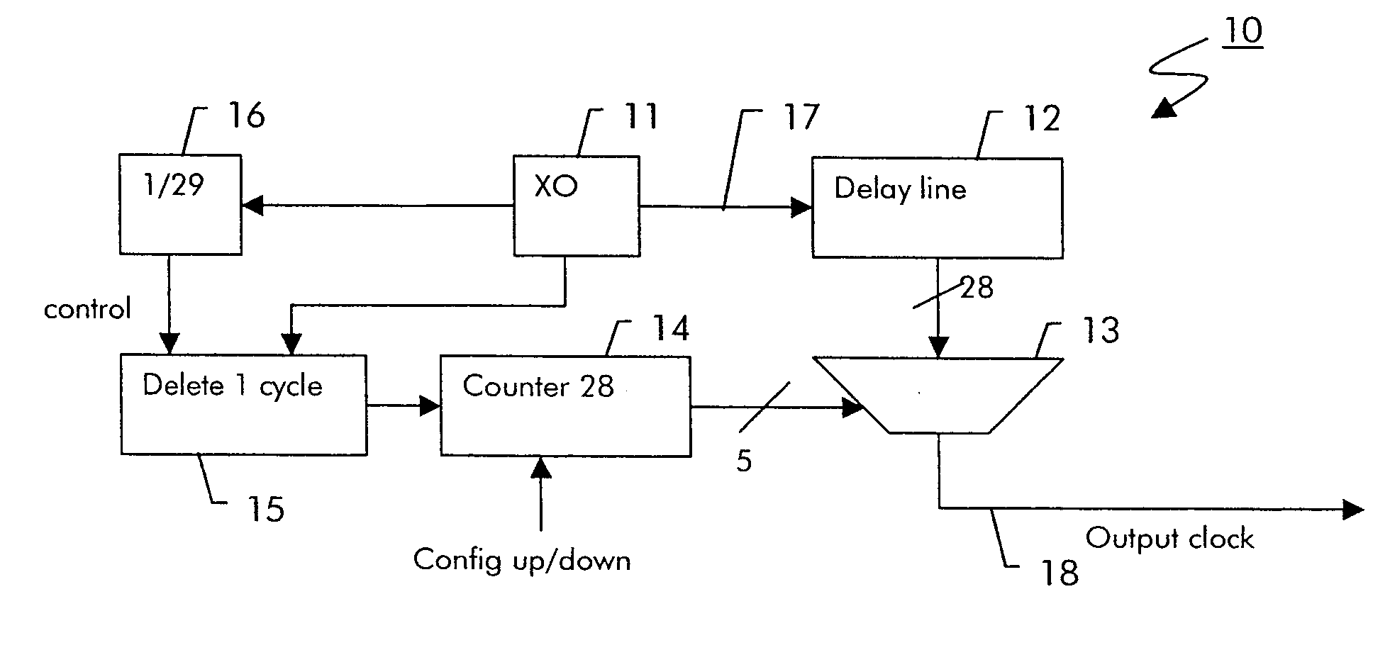
[0017]Clock filter circuits are used on the I / O boards of a network element for a transport network. It serves to filter the data clock of payload channels contained in the transport signals to be sent. In the preferred embodiment, each I / O board receives 16 payload channels from the switch matrix of the network element. These channels are then de-mapped from an internal transport frame. Due to the removal of the stuff bits, the de-mapped payload channels are provided at a gapped clock. The clock filter circuit smoothes these gaps and generates a transmit line signal with low intrinsic jitter to meet the requirements defined in the applicable standards. Each payload channel has its own individual clock signal.

[0018]On the I / O board, each payload channel coming from the matrix is (after de-mapping from the internal frame) written to a buffer memory at its gapped payload bit clock and read back from the buffer using a filtered read clock. The clock filter circuit that generates the fi...


PUM


Abstract

A clock filter circuit (20), which serves for filtering the clock of non-isochronous data signals having a selected one of at least two nominal data rates, has an auxiliary clock source (21) that generates an auxiliary clock signal (27) with a pulse repetition rate which is in the range between the at least two predetermined data rates, a delay line (22) connected to the auxiliary clock source (21) for creating a set of mutually delayed copies of the auxiliary clock signal and a multiplexer (23) that switches in a cyclic order between the delayed copies according to predetermined rules, which depend on the selected data rate to generate a filtered clock signal (28). A control circuit determines whether the rate of the filtered clock (28) signal must be increased or decreased as compared to said data signal and controls the multiplexer (23) to delay or advance the cyclical switching accordingly.

Description

[0001]The invention is based on a priority application EP04 293 123.8 which is hereby incorporated by reference.FIELD OF THE INVENTION[0002]The present invention relates to the field of telecommunications and more particularly to a digital clock filter circuit for a gapped clock of a non-isochronous data signal and a method of filtering a clock signal of a non-isochronous data signal.BACKGROUND OF THE INVENTION[0003]Network elements in existing transport networks serve for establishing semi-permanent (“cross”)connections in the network. Such network elements include crossconnects and add / drop multiplexers. For crossconnecting high bitrate digital signals, it is advantageous to use a synchronous switch matrix. While today transport networks rely basically on the Synchronous Digital Hierarchy (SDH, ITU-T G.707), a new Optical Transport Hierarchy has been defined in ITU-T G.709, where the transport signals are no longer synchronous but asynchronous within a predetermined range of ±20 p...

Claims


Application Information

Patent Timeline
Patent Type & Authority Patents(United States)
IPC IPC(8): G06F1/04
CPCH04J3/076H03L7/0814H03L7/0816
Inventor WOLF, MICHAEL JOACHIMTHIELE, WOLFGANG
Owner ALCATEL LUCENT SAS
Why Eureka
Try Eureka