Photoelectric conversion device and image sensor

a conversion device and photoelectric technology, applied in the direction of semiconductor devices, basic electric elements, electrical appliances, etc., can solve the problems of reducing the manufacturing steps and resulting cost, conductive contaminant may be stuck to the upper surface, and reducing the sensitivity, so as to prevent the reduction of the sensitivity of the photodiode, reduce the manufacturing time, and suppress the increase in capacitance

Inactive Publication Date: 2010-04-27
ABLIC INC
View PDF4 Cites 0 Cited by
  • Summary
  • Abstract
  • Description
  • Claims
  • Application Information

AI Technical Summary

Benefits of technology

[0009]The present invention has been made in view of the above-mentioned circumstances. An object of the present invention is to provide a photoelectric conversion device capable of reducing a manufacturing cost and preventing a reduction in sensitivity of a photodiode caused by an increase in effective capacitance thereof even when a conductive contaminant or the like is stuck to an upper surface of a interconnecting portion during a manufacturing process, and an image sensor including the photoelectric conversion device.
[0012]According to the aspects of the present invention, formation of the organic film by the thermoplastic polyimide resin containing conductive particles or conductive fibers enables the setting of the thickness of the organic film to approximately 2 μm to 10 μm, resulting in the large distance between an upper surface of the organic film and an upper surface of the interconnecting line of the interconnecting portion in the photoelectric conversion device. In the pixel region of a photodiode formed as a light receiving element by a semiconductor PN junction, it is thus possible to suppress the increase in capacitance, which is caused by sticking of conductive contaminants or the like to the upper surface of the organic film, preventing the reduction in sensitivity of the photodiode. In addition, formation of the organic film of the polyimide resin enables reduction in, for example, a time necessary to form a second-layer metal film and to etch this film as compared with that in the case where a conductor made of only a metal material is used, reducing manufacturing time thereof, and also manufacturing cost thereof.
[0013]According to the photoelectric conversion device and the image sensor of the present invention, the manufacturing cost can be reduced. In addition, even when the conductive contaminant or the like is stuck to the upper surface of the organic film during the manufacturing process, the reduction in sensitivity of the photodiode caused by the increase in capacitance thereof can be prevented.

Problems solved by technology

Since the electrical conductor is, however, made of the metal material according to the conventional photoelectric conversion device, a pattern made of two metal materials for two layers, one for an interconnecting line of the interconnecting portion and the other for the electrical conductor, is provided in the photoelectric conversion device, making it difficult to reduce a manufacturing steps and resulting cost thereof.
During a process for manufacturing the photoelectric conversion device, for example, a conductive contaminant may be stuck to an upper surface of the interconnecting portion.
Presence of a parasitic capacitance caused between the interconnecting portion and the conductive contaminant in parallel to a capacitance of the photodiode increases an effective capacitance of the photodiode, which reduces the sensitivity thereof.

Method used


Image

  • Photoelectric conversion device and image sensor
  • Photoelectric conversion device and image sensor

Examples


Embodiment Construction

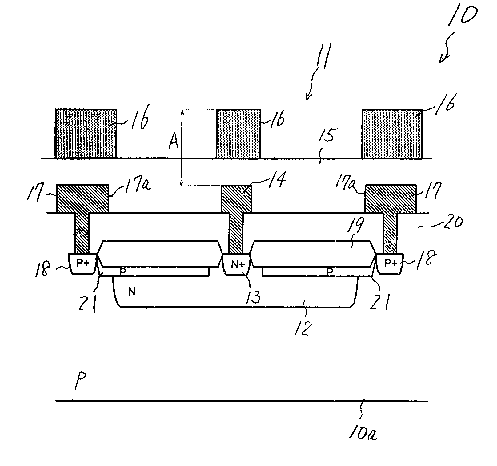
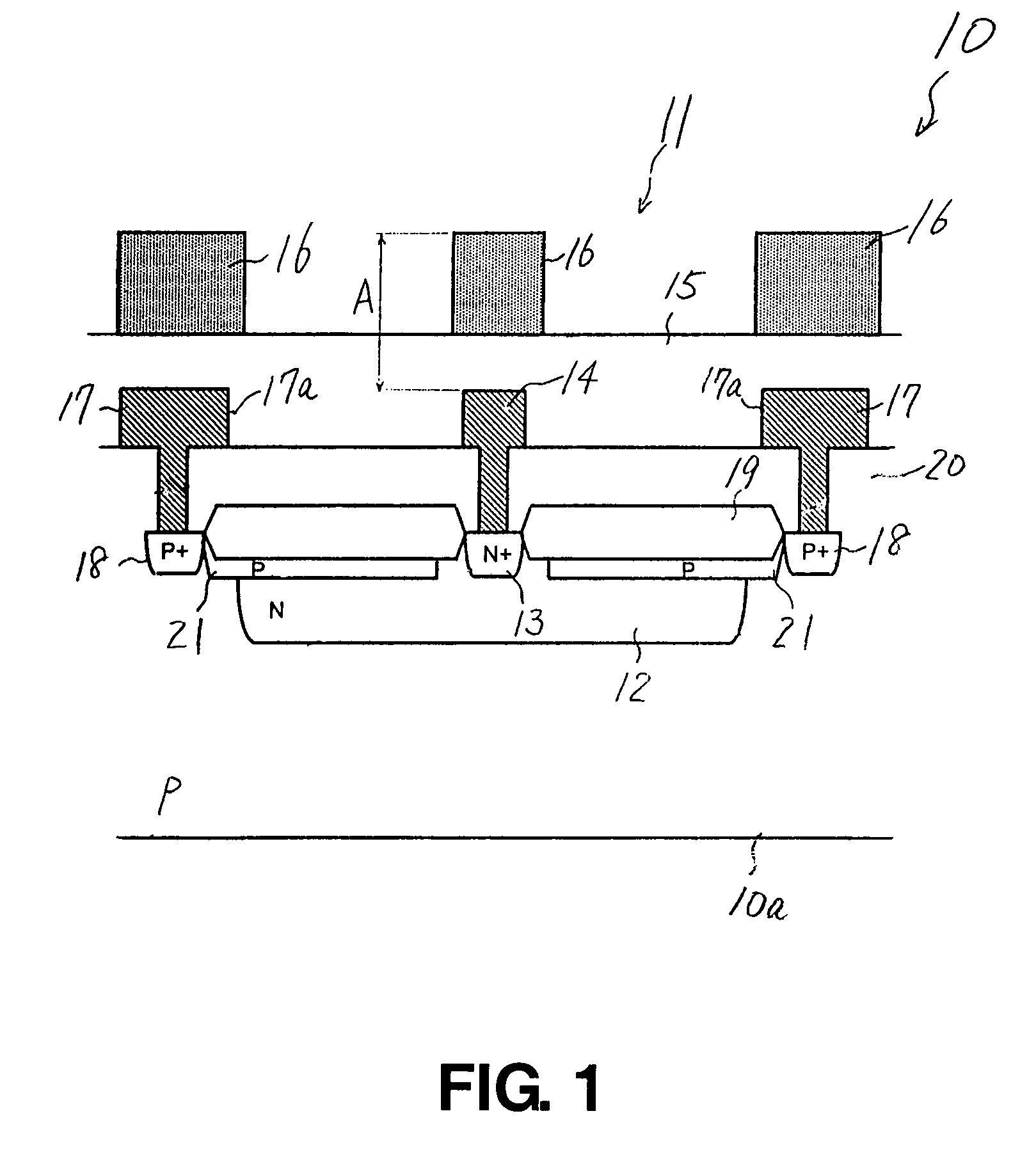
[0015]Hereinafter, an embodiment of the present invention will be described with reference to FIG. 1. A photoelectric conversion device 10 according to this embodiment includes a first conductivity type semiconductor substrate (first semiconductor region) 10a, a second conductivity type semiconductor region (second semiconductor region) 12 provided in a pixel region 11 of the semiconductor substrate 10a, for storing a signal charge, interconnecting portions 13 and 14 for connecting the semiconductor region 12 with a circuit element (not shown) provided outside the pixel region 11, and an organic film 16 provided above a portion of the interconnecting portions 13 and 14 located in the pixel region 11 through an insulating protective film 15.

[0016]In the example shown in FIG. 1, the semiconductor substrate 10a is set as a P-type region and the semiconductor region 12 is set as an N-type region. A light-shielding layer 17 is provided on a surface side of the semiconductor substrate 10a...


PUM


Abstract

A photoelectric conversion device (10) includes a first conductivity type first semiconductor region (10a) located in a pixel region (11), a second conductivity type second semiconductor region (12) provided in the first semiconductor region (10a), for storing a signal charge, interconnecting portions (13 and 14) for connecting the second semiconductor region (12) with a circuit element provided outside the pixel region (11), and an organic film (16) which is provided above a portion located in the pixel region (11) in the interconnecting portions (13 and 14) through an insulating protective film (15) and held at a predetermined potential. The organic film (16) is made of a thermoplastic polyimide resin containing one of a conductive particle and a conductive fiber.

Description

[0001]This application claims priority under 35 U.S.C. §119 to Japanese Patent Application No. JP2006-057549 filed Mar. 3, 2006, the entire content of which is hereby incorporated by reference.BACKGROUND OF THE INVENTION[0002]1. Field of the Invention[0003]The present invention relates to a photoelectric conversion device and an image sensor.[0004]2. Description of the Related Art[0005]As for an example of photoelectric conversion device, there is known a structure as described in, for example, JP 2000-311997 A, which includes a first semiconductor region of a first conductivity type located in a pixel region, a second semiconductor region of a second conductivity type provided in the first semiconductor region for storing a signal charge, a interconnecting portion for connecting the second semiconductor region with a circuit element provided outside the pixel region, and an electrical conductor which is provided above a portion located in the pixel region in the interconnecting por...

Claims


Application Information

Patent Timeline
Patent Type & Authority Patents(United States)
IPC IPC(8): H01L29/78
CPCH01L27/14636
Inventor OMI, TOSHIHIKO
Owner ABLIC INC
Why Eureka
Try Eureka