Solid imaging device

A solid-state imaging device, pixel technology, applied in radiation control devices, signal generators with a single pickup device, image communication, etc., can solve the problem of reduced storage time, fewer photoelectric conversion elements, and shorter storage time. problem, to prevent the reduction of sensitivity, to achieve high image quality, and to achieve the effect of high practical value

Active Publication Date: 2007-05-09
GK BRIDGE 1
View PDF1 Cites 6 Cited by
  • Summary
  • Abstract
  • Description
  • Claims
  • Application Information

AI Technical Summary

Problems solved by technology

[0006] However, in conventional solid-state imaging devices, memories for storing pixel signals are connected in parallel, and pixel mixing is performed by averaging. Therefore, the pixel signals are not added together, but the average value of the pixel signals is output.
Here, in the case of the still image mode, since each photoelectric conversion element is read separately, the storage time is long and the amount of light is large, resulting in a high output signal, but in the case of the moving image mode, since the The signal of the photoelectric conversion element is mixed at a high speed in units, so the number of photoelectric conversion elements with practical effects becomes smaller, and in practice, the storage time becomes shorter
Therefore, in the conventional solid-state imaging device, the amount of light decreases and the output signal value is not added, so the output signal value decreases in proportion to the shortened storage time, resulting in a decrease in sensitivity

Method used


Image

  • Solid imaging device
  • Solid imaging device
  • Solid imaging device

Examples


Embodiment approach 1

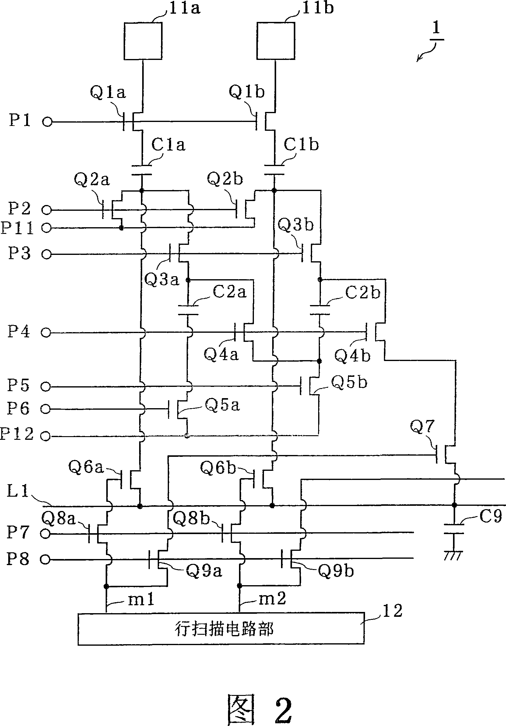
[0062] FIG. 2 is a schematic diagram showing the circuit configuration of the solid-state imaging device according to the first embodiment. In addition, the example shown in this figure shows the case where there are two pixel parts (photoelectric conversion elements) arranged in the row direction.

[0063] As shown in FIG. 2, the solid-state imaging device 1 includes: pixel sections 11a and 11b; a plurality of MOS transistors Q1a, Q1b, Q2a, Q2b, Q3a, Q3b, Q4a, Q4b, Q5a, Q5b, Q6a, Q6b, Q7, Q8a, Q8b, Q9a, Q9b; a plurality of capacitors C1a, C1b, C2a, C2b; row scanning circuit section 12; drive pulse application terminals P1, P2, P3, P4, P5, P6, P7, P8 to which drive pulse application terminals Drive pulses from the column scanning circuit section or signal readout circuit section not shown; bias voltage application terminals P11 and P12 to which the bias voltage from the column scanning circuit section or the signal readout circuit section is applied ; And the signal output li...

Embodiment approach 2

[0099] Next, another solid-state imaging device according to the present invention will be described.

[0100] FIG. 7 is a circuit diagram showing the configuration of the solid-state imaging device shown in the second embodiment. Here, as described above, in the solid-state imaging device 1, since the signal value output to the signal output line L1 is divided by the capacitor C9, there is a loss.

[0101] Therefore, as shown in FIG. 7 , the solid-state imaging device 2 according to the second embodiment includes, in addition to the structure of the solid-state imaging device 1, a high input impedance circuit 13 connected to the MOS transistor Q4b between the source and the drain of the MOS transistor Q7.

[0102] As a result, the value of the signal output to the signal output line L1 is not divided by the capacitor C9, and in the case of the memory circuit having the two structures of FIG. 7, the signal value is 2*Vt, and in the case of having N memory circuits Next, the ...

Embodiment approach 3

[0110] Next, another solid-state imaging device of the present invention will be described.

[0111] 9 is a circuit diagram showing the configuration of the solid-state imaging device according to the third embodiment. As shown in FIG. 9 , the solid-state imaging device 3 is applicable when two pixel sections (photoelectric conversion elements) are arranged in the column direction, and the solid-state imaging device 3 includes pixel sections 30 a and 30 b , and MOS transistors Q1 , Q2 , and Q6 . , Q11a, Q11b, Q12a, Q12b, Q13a, and Q13b; capacitors C1, C3a, C3b; buffer 31; row scanning circuit section 32; Pressure application terminals P31 and P32; and signal output lines L2 and L3, etc.

[0112] The pixel portions 30a and 30b include a photoelectric conversion element, a charge transfer portion, a charge-to-voltage conversion portion, a voltage amplifying portion, and the like. In FIG. 9, the detailed circuit configuration of the pixel sections 30a and 30b is omitted.

[01...


PUM


Abstract

The present invention provides a solid-state imaging device in which sensitivity is prevented from lowering even when signals of pixels are mixed. The solid-state imaging device 1 includes a plurality of pixel units 11 and 11b each of which has a photoelectric conversion element, and is capable of summing signals corresponding to respective outputs of the photoelectric conversion elements of the pixel units. The device includes: a plurality of capacitors C2a and C2b, each of which individually accumulates electric charges corresponding to a signal outputted from the associated photoelectric conversion element; and a plurality of MOS transistors Qa and Qb which are alternately connected with the associated capacitor C2a or C2b. By disconnecting the MOS transistor Qa or Qb, the electric charges of the signal outputted from each of the photoelectric conversion elements are accumulated in each associated capacitor C2a or C2b, and by conducting the MOS transistors Qa and Qb to sum the signals of the pixel units, the capacitors C2a and C2b are connected in series.

Description

technical field [0001] The present invention relates to a MOS type solid-state imaging device used in a digital camera and the like, and particularly relates to a technique effective for pixel addition (pixel addition). Background technique [0002] In recent years, solid-state imaging devices have become more and more pixel-intensive, and have grown to 5 million pixels, etc., and it is possible to capture even still images at the level of silver halide cameras, and it is also possible to capture moving images. Here, since a moving image is shot with hundreds of thousands of pixels, in order to effectively utilize the rest of the photoelectric conversion elements, a method of pixel-mixing the signal of each photoelectric conversion element is generally employed (for example, Patent Document 1). [0003] FIG. 1 is a schematic diagram showing the structure of a signal readout circuit of a conventional solid-state imaging device. As shown in FIG. 1 , the signal readout circui...

Claims


Application Information

Patent Timeline
Patent Type & Authority Applications(China)
IPC IPC(8): H04N5/335H01L27/146H04N5/347H04N5/374H04N5/378H04N9/07
CPCH04N3/1562H04N25/46H04N25/76
Inventor 村田隆彦山口琢己春日繁孝
Owner GK BRIDGE 1
Why Eureka
Try Eureka