Techniques for grouping circuit elements into logic blocks

a technology of logic blocks and circuit elements, applied in the field of logic block grouping circuits, can solve the problems of violating design rules, unable to separate the lut and register of the placement tool, and affecting the routability and timing of the logic block, so as to improve the routability of the design and signal timing

Inactive Publication Date: 2010-04-27
ALTERA CORP
View PDF11 Cites 5 Cited by
  • Summary
  • Abstract
  • Description
  • Claims
  • Application Information

AI Technical Summary

Benefits of technology

[0014]Individual abstract blocks can be separated and moved independently of other circuits that were previously grouped into the same logic block. For example, a LUT and register that were previously placed into the same logic block can be separated. The LUT and the register can be placed into different logic blocks to further improve routability of the design and signal timing.

Problems solved by technology

During placement, routability and timing issues between logic blocks become apparent that were not apparent during synthesis.
However, a placement tool cannot separate the LUT and register without potentially violating design rules of the FPGA.

Method used


Image

  • Techniques for grouping circuit elements into logic blocks
  • Techniques for grouping circuit elements into logic blocks
  • Techniques for grouping circuit elements into logic blocks

Examples


Embodiment Construction

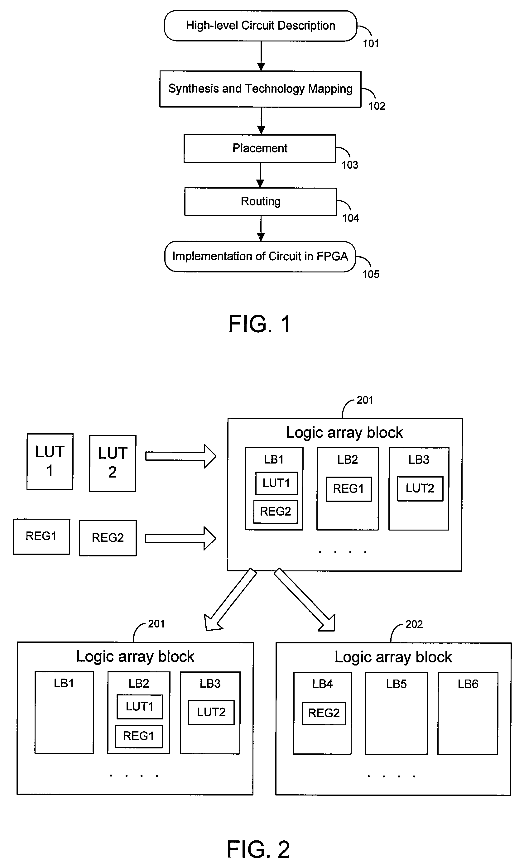
[0023]FIG. 1 is flow chart that illustrates a generalized process for mapping a user made circuit design to a programmable integrated circuit (IC) such as an FPGA or a PLD. The first step 102 in this mapping process involves synthesis and technology mapping. During synthesis and technology mapping, networks of logic gates in a user circuit design 101 are converted into circuit elements that can be placed into a programmable IC. The logic gates can be converted into various types of circuit elements such as lookup tables (LUTs), registers, RAM, and digital signal processing (DSP) blocks, depending on the particular programmable IC architecture.

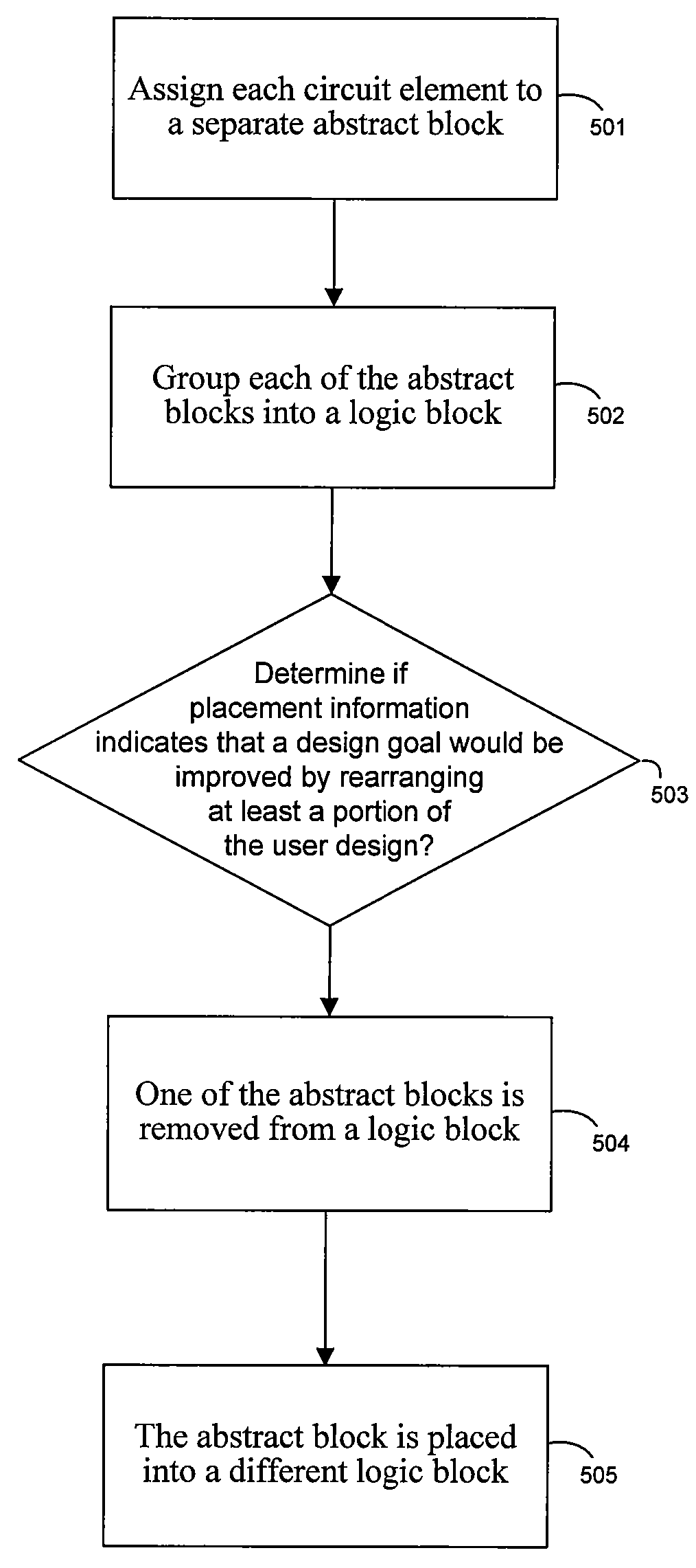
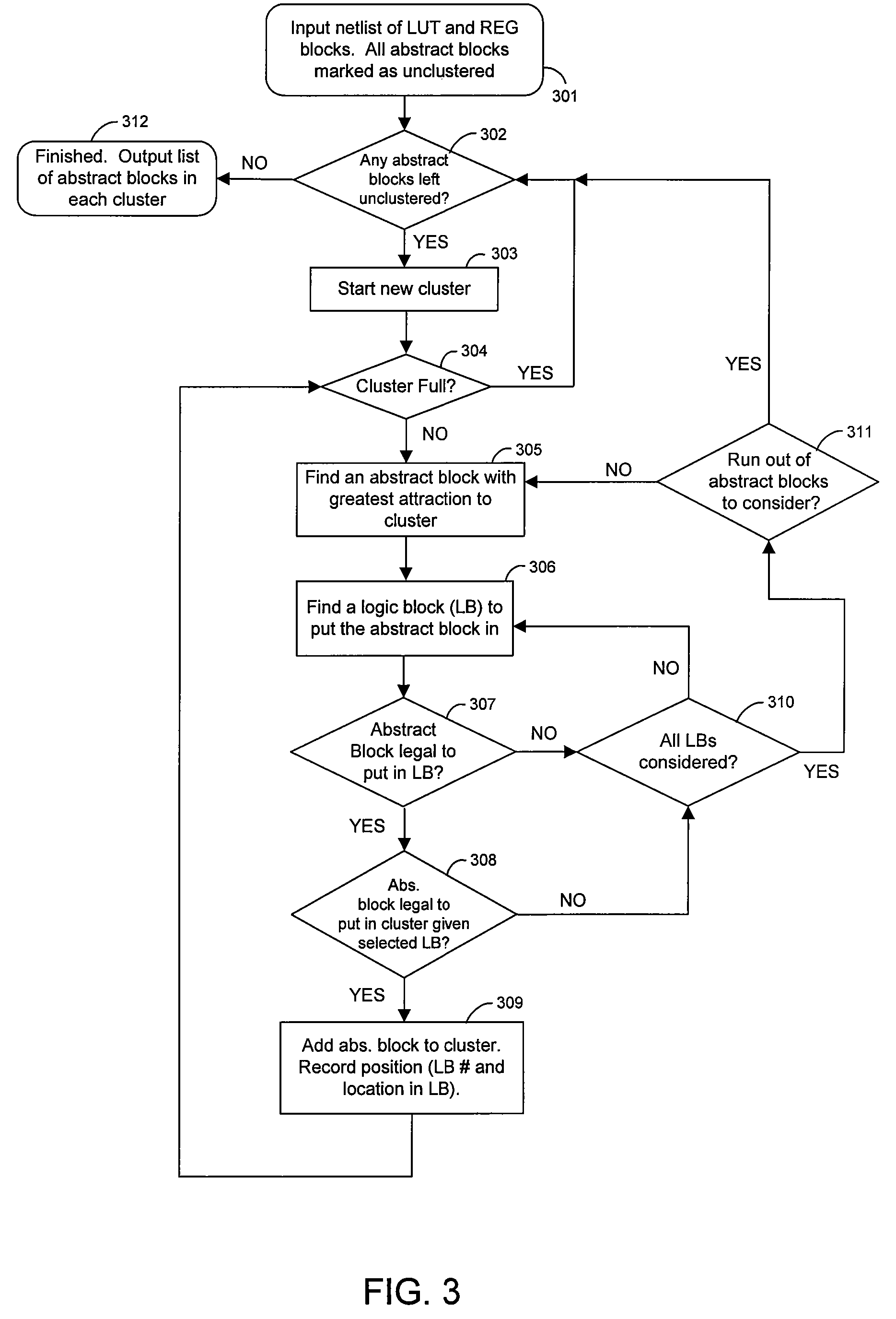
[0024]During placement step 104, a packing tool of the present invention groups the LUTs, registers, and other circuit blocks generated during technology mapping into logic blocks. Each logic block typically includes at least one LUT and at least one register. Logic blocks can be grouped into clusters of logic blocks such as a LAB on a programm...


PUM


Abstract

Techniques are provided for grouping circuits in a user design for a programmable integrated circuit into logic blocks. A packing tool separates each circuit element into individual abstract blocks and groups the abstract block into logic blocks. A determination is made whether placement information indicates that a design goal would be improved by rearranging at least a portion of the user design. The user design can be rearranged by moving one or more of the abstract blocks into different logic blocks than the ones they were previously grouped with. Circuit elements in the same logic block can be separated and placed into different logic blocks to improve routability of the user design and signal timing.

Description

CROSS-REFERENCES TO RELATED APPLICATIONS[0001]The present application is a continuation of U.S. Pat. No. 7,275,228, granted Sep. 25, 2007, and entitled “TECHNIQUES FOR GROUPING CIRCUIT ELEMENTS INTO LOGIC BLOCKS”, and is herein fully incorporated by reference for all purposes.BACKGROUND OF THE INVENTION[0002]The present invention relates to techniques for grouping circuits into logic blocks, and more particularly, to techniques for grouping lookup tables, registers and other circuits into logic blocks that allow the circuits to be separated and moved independently during placement of a circuit design for a programmable integrated circuit.[0003]A field programmable gate array (FPGA) is a programmable integrated circuit. Programmable integrated circuits also include programmable logic devices (PLDs), programmable logic arrays (PLAs), configurable logic arrays, etc. Many programmable integrated circuits are hybrids of FPGAs and ASICs (application specific integrated circuits).[0004]Pro...

Claims


Application Information

Patent Timeline
Patent Type & Authority Patents(United States)
IPC IPC(8): G06F17/50G06F9/45
CPCG06F17/505Y02T10/82G06F17/5077G06F17/5072G06F30/327G06F30/392G06F30/394
Inventor PADALIA, KETANBOZMAN, KIMBERLYBETZ, VAUGHN
Owner ALTERA CORP
Why Eureka
Try Eureka