Embedded capacitor structure in circuit board and method for fabricating the same

a capacitor and capacitor structure technology, applied in the direction of printed capacitor incorporation, printed circuit aspects, printed electric components, etc., can solve the problems of limiting the number of passive components capable of being mounted on the substrate, affecting the trace routability of the substrate, and not being favorable for the development of highly integrated packages, so as to achieve effective filling of spaces, ensure the reliability of the circuit board, and improve the fluidity

Inactive Publication Date: 2006-03-23
PHOENIX PRECISION TECH CORP
View PDF4 Cites 0 Cited by
  • Summary
  • Abstract
  • Description
  • Claims
  • Application Information

AI Technical Summary

Benefits of technology

[0007] In view of the above, a primary objective of the present invention is to provide an embedded capacitor structure in a circuit board and a method for fabricating the same, which can assure planarity and reliability of the circuit board, increase the number of passive components incorporated in a semiconductor package using the circuit board, and improve trace routability on the circuit board.
[0010] By the above embedded capacitor structure in a circuit board and the method for fabricating the same according to the invention, prior to applying a capacitive material over the circuit board, a dielectric layer is formed on and made flush with a first circuit layer patterned on the circuit board, wherein the first circuit layer has at least one first electrode plate for the capacitor structure. The dielectric layer is made of a material having a lower dielectric constant and better fluidity than those of the capacitive material, such that it can effectively fill the spaces between patterned traces of the first circuit layer without leaving unfilled gaps, which thereby assures the reliability of the circuit board and prevents delamination between laminated layers of the circuit board. The flush arrangement of the dielectric layer and the first circuit layer provides good planarity for subsequent build-up layers formed thereon. After the capacitive material is deposited on the dielectric layer and the first circuit layer, a second circuit layer is formed on the capacitive material and has at least one second electrode plate corresponding in position to the first electrode plate, together with the capacitive material disposed in-between, to form the capacitor structure embedded in the circuit board. The embedded arrangement of capacitor does not affect trace routability nor occupy area on the surface of the circuit board, thereby increasing flexibility of the number of capacitors capable of being incorporated in the circuit board and improving the trace routability on the circuit board.

Problems solved by technology

However by this arrangement, the passive components not only occupy the surface area of the substrate but also adversely affect the trace routability on the substrate; besides, certain surface area of the substrate is reserved for bond pads, which thus limits the number of passive components capable of being mounted on the substrate, and is not favorable for development of highly integrated packages.
Further, in the case of more passive components required for a performance-enhanced package, the substrate needs to be enlarged to accommodate the plurality of passive components and semiconductor chips, such that the package size would be significantly increased and not compliant with the trend of profile miniaturization.
However, when the capacitive material e.g. polymer is applied over the circuit layer, the polymeric material having poor fluidity can hardly effectively fill the spaces between adjacent traces of the circuit layer thereby leaving unfilled gaps, such that the thickness of the capacitive or polymeric material is not easily made even, making a subsequent circuit layer formed thereon not having good planarity.
Those drawbacks not only degrade the electrical performance of a fabricated circuit board, but also affect the reliability of a subsequently formed build-up structure for a circuit board.

Method used


Image

  • Embedded capacitor structure in circuit board and method for fabricating the same
  • Embedded capacitor structure in circuit board and method for fabricating the same
  • Embedded capacitor structure in circuit board and method for fabricating the same

Examples


Embodiment Construction

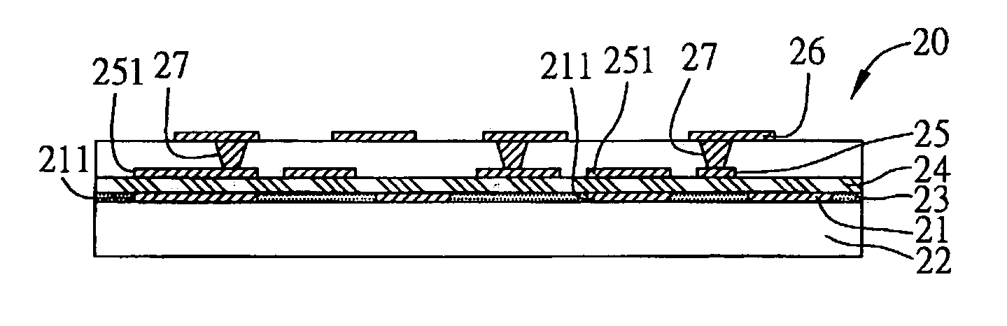
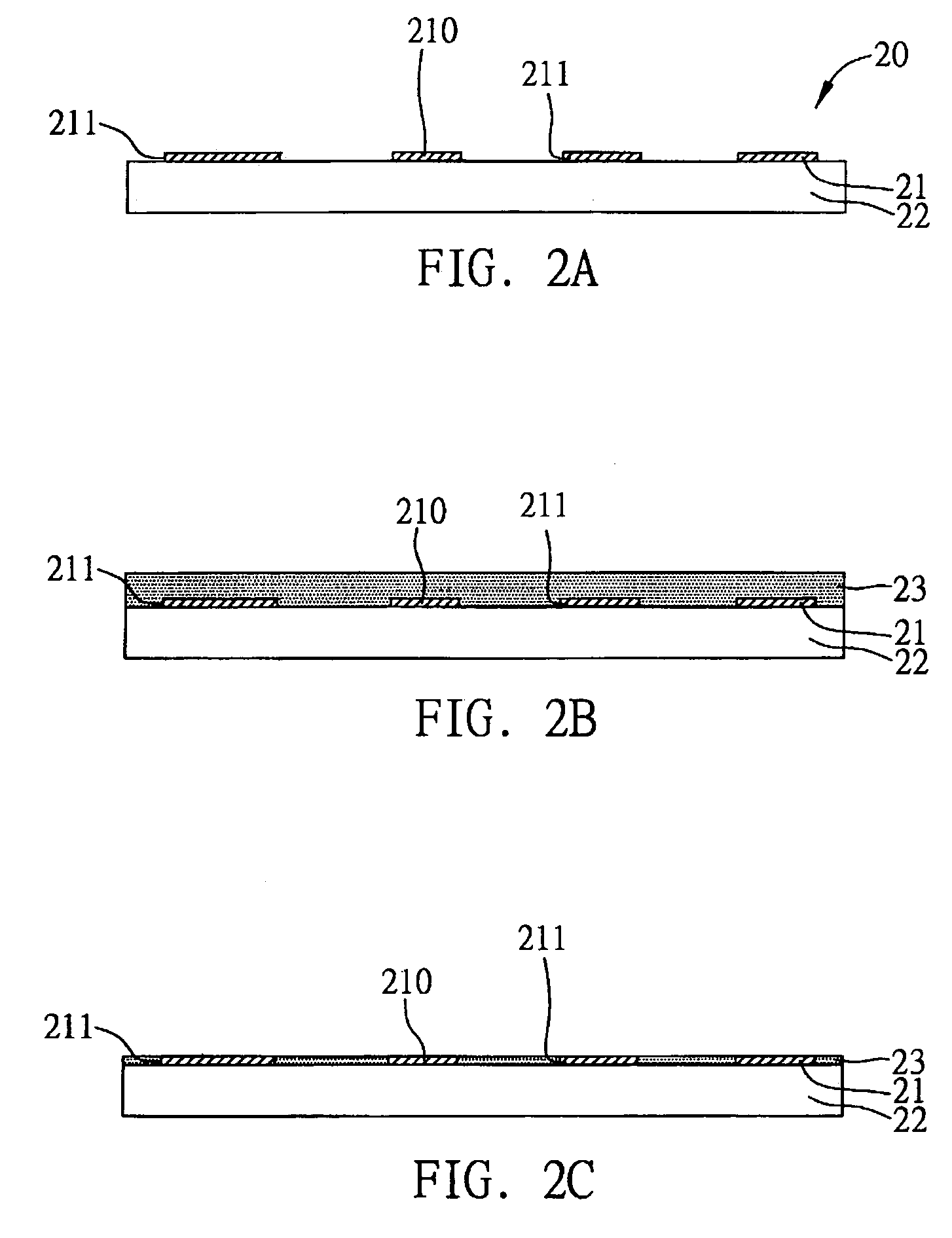
[0014] The preferred embodiment of the present invention is described in detail with reference to FIGS. 2A through 2F.

[0015]FIGS. 2A through 2F illustrates the steps of a method for fabricating an embedded capacitor structure in a circuit board 20 according to the invention.

[0016] Referring to FIG. 2A, the first step is to provide the circuit board 20 formed with a first circuit layer 21 on at least one surface thereof, wherein the first circuit layer 21 comprises a plurality of patterned traces 210, and a plurality of trace regions serving as first electrode plates 211 for the capacitor structure. The circuit board 20 is primarily composed of an insulating layer 22 made of epoxy resin, polyimide resin, cyanate ester, glass fiber, BT (bismaleimide triazine) resin, a mixture of insulating organic materials (such as epoxy resin and glass fiber), or ceramics.

[0017] With reference to FIG. 2B, a dielectric layer 23 is formed on the insulating layer 22 and the first circuit layer 21. T...


PUM

PropertyMeasurementUnit
dielectricaaaaaaaaaa
dielectric constantaaaaaaaaaa
operating speedaaaaaaaaaa

Abstract

An embedded capacitor structure in a circuit board and a method for fabricating the same are proposed. The circuit board is formed with a first circuit layer on at least one surface thereof, wherein the first circuit layer has at least one first electrode plate for the capacitor structure. Then, a dielectric layer is formed on the first circuit layer and made flush with the first circuit layer. The dielectric layer has a relatively low dielectric constant and good fluidity to effectively fill the spaces between patterned traces of the first circuit later. A capacitive material is deposited on the dielectric layer and the first circuit layer. Finally, a second circuit layer is formed on the capacitive material and has at least one second electrode plate corresponding to the first electrode plate, together with the capacitive material disposed in-between, to form the capacitor structure.

Description

FIELD OF THE INVENTION [0001] This application is a divisional of application Ser. No. 10 / 739,371 filed Dec. 17, 2003 and claims priority of Taiwan Application No. 092128802 filed Oct. 17, 2003. [0002] The present invention relates to embedded capacitor structures in circuit boards and methods for fabricating the same, and more particularly, to a film of capacitive material embedded in a semiconductor package substrate, and a method for forming the capacitor structure. BACKGROUND OF THE INVENTION [0003] In order to achieve desirable functionality and operating speed of electronic devices, semiconductor packages used therein are usually incorporated with passive components, such as resistors, capacitors and inductors, for enhancing and stabilizing performances of the electronic devices. The passive components are typically mounted on a surface of a circuit board such as printed circuit board or semiconductor package substrate, wherein the passive components can be located at corners ...

Claims


Application Information

Patent Timeline
Patent Type & Authority Applications(United States)
IPC IPC(8): H01L21/8242H01L23/498H05K1/03H05K1/16H05K3/46
CPCH01L23/49822H01L2924/09701H05K1/0306H05K1/162H05K3/4644H05K2201/0209Y10T29/417H05K2201/09881H01L2924/0002H05K2201/09672Y10T29/435H01L2924/00
Inventor CHANG, RUEI-CHIH
Owner PHOENIX PRECISION TECH CORP
Why Eureka
Try Eureka