Chip and power planning method

a power planning and chip technology, applied in the field of power planning, can solve the problems of increasing the dynamic power of the power supply, increasing the difficulty of power supply, so as to facilitate the connection of macros, increase the effective power stripe width, and increase the routability

Active Publication Date: 2020-03-03
NCKU RES & DEV FOUND +1
View PDF1 Cites 0 Cited by
  • Summary
  • Abstract
  • Description
  • Claims
  • Application Information

AI Technical Summary

Benefits of technology

[0006]In view of the foregoing, it is an object of the embodiment of the present invention to provide a routability-driven macro-aware power planning method and chip that is capable of substantially increasing routability and facilitating connection of macros according to their locations; proposing an effective power stripe width which can substantially increase overall effectiveness of routing resource; and providing a more precise cost function to determine locations of power stripes in a region based on dynamic programming algorithm.

Problems solved by technology

As performance of a design continuously improves, a modern chip consumes larger dynamic power, which makes voltage drop a serious problem.
The problem becomes even more tough when lower supply voltages are used to reduce dynamic power of ICs because a tolerable voltage drop value is further shrunk.
Because all macros have to be connected to a power / ground network, power planning becomes more complex than ever.
With the number of macros in a modern SoC increases dramatically, it is ineffective to rely on experienced designers to perform power planning manually.

Method used


Image

  • Chip and power planning method
  • Chip and power planning method
  • Chip and power planning method

Examples


Embodiment Construction

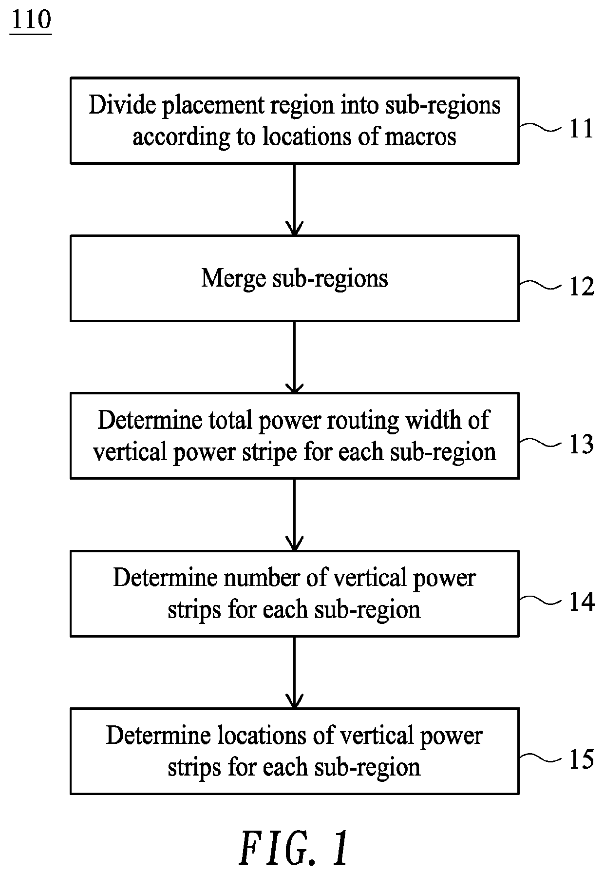
[0016]FIG. 1 shows a flow diagram illustrating a routability-driven macro-aware power planning method (“power planning method” hereinafter) 100 according to one embodiment of the present invention.

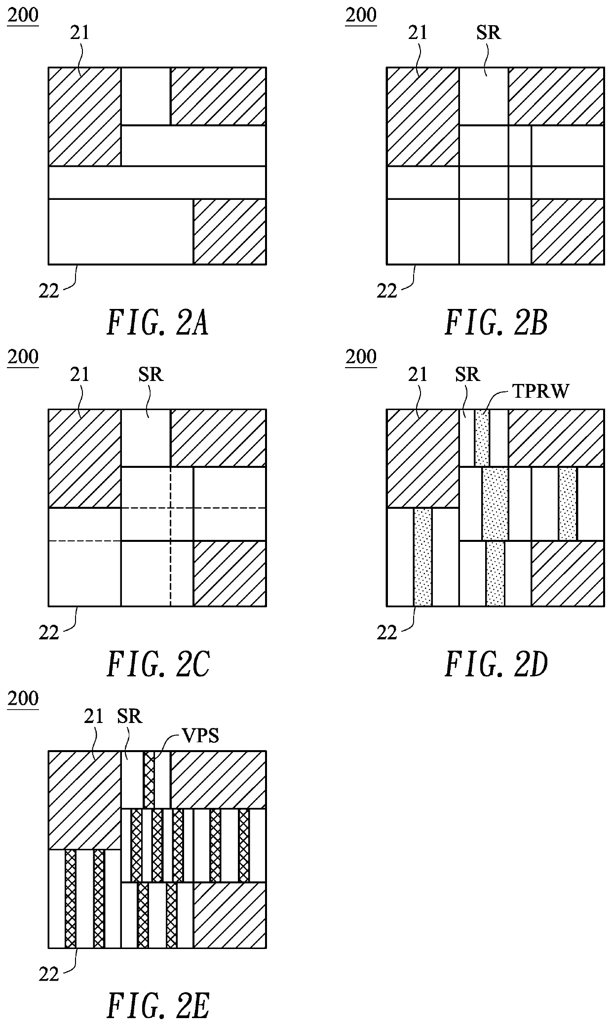
[0017]In step 11, a placement region of a chip may be divided into a plurality of sub-regions (SRs) according to locations of macros. In the specification, the term chip (or microchip) refers to an integrated circuit that is composed of electronic circuits such as intellectual property (IP) cores or macros placed on a semiconductor (e.g., silicon) substrate. FIG. 2A schematically shows a top view illustrating a chip 200 having macros 21 (denoted by hatched region) that are placed beforehand (i.e., pre-placed) within a placement region 22.

[0018]Specifically, as shown in FIG. 2A, for each macro 21, a first horizontal line overlapping a horizontal power stripe (HPS) nearest (but not necessarily coinciding with) a top edge of the macro 21 is extended until bumping into another macro or a bound...


PUM


Abstract

A chip includes a substrate; macros placed on the substrate, which has a placement region being divided into sub-regions according to locations of the macros; and one or more vertical power stripes (VPSs) disposed in each sub-region. At least one VPS is not aligned with the VPSs of an adjacent higher or lower sub-region.

Description

BACKGROUND OF THE INVENTION1. Field of the Invention[0001]The present invention generally relates to power planning, and more particularly to a routability-driven macro-aware power planning method and chip.2. Description of Related Art[0002]Power planning has become a very important step in the physical design of an integrated circuit (IC). Due to shrinking of a feature size, a unit area in a chip contains more and more electronic components, which make power density in a chip increase dramatically. As performance of a design continuously improves, a modern chip consumes larger dynamic power, which makes voltage drop a serious problem. The problem becomes even more tough when lower supply voltages are used to reduce dynamic power of ICs because a tolerable voltage drop value is further shrunk.[0003]In order to provide stable and stronger power to devices, power is usually delivered through a global power mesh before it can reach macros or standard cells. A power mesh, which consists...

Claims


Application Information

Patent Timeline
Patent Type & Authority Patents(United States)
IPC IPC(8): G06F30/392G06F30/394
CPCG06F30/394G06F30/392G06F2119/06
Inventor LIN, JAI-MINGSYU, JHIH-SHENGHUANG, BO-YUAN
Owner NCKU RES & DEV FOUND
Why Eureka
Try Eureka