Semiconductor device having multi-layer wiring

a semiconductor and multi-layer technology, applied in the direction of transistors, optics, instruments, etc., can solve the problems of difficult to ensure the selective ratio between the film of an organic material and the resist mask, low selectivity ratio, and difficulty in forming contact holes, etc., to achieve excellent contact properties and low resistance

Inactive Publication Date: 2005-03-01
SEMICON ENERGY LAB CO LTD
View PDF25 Cites 170 Cited by
  • Summary
  • Abstract
  • Description
  • Claims
  • Application Information

AI Technical Summary

Benefits of technology

It is possible to use a conductive material as the first metallic layer or the second metallic layer in the aforementioned configurations. For example, a material layer predominantly is composed of Al, Ta, Ti, Cr, W, Mo or silicon provided with conductivity, or multi-layer film comprised thereof can be used. Furthermore, the first metallic layer is preferably composed of aluminum, which has low resistance, and a material predominantly composed of aluminum.
Furthermore, the aforementioned second metallic layer is preferably composed of titanium, which has an excellent contact property, and a material predominantly composed of titanium.

Problems solved by technology

Where the dry etching method is used, since the silicon oxide film and the semiconductor layer predominantly composed of silicon have the same main ingredient, such a problem was present in that the selective ratio was low and the semiconductor layer, which is thin in thickness, was stripped off at the same time.
Conventionally, in the case where a resist mask was used in the dry etching method, since the mask has a similar constituent, it was difficult to ensure the selective ratio between the film of an organic material and the resist mask and thus contact holes were formed with difficulty.

Method used


Image

  • Semiconductor device having multi-layer wiring
  • Semiconductor device having multi-layer wiring
  • Semiconductor device having multi-layer wiring

Examples


embodiment 1

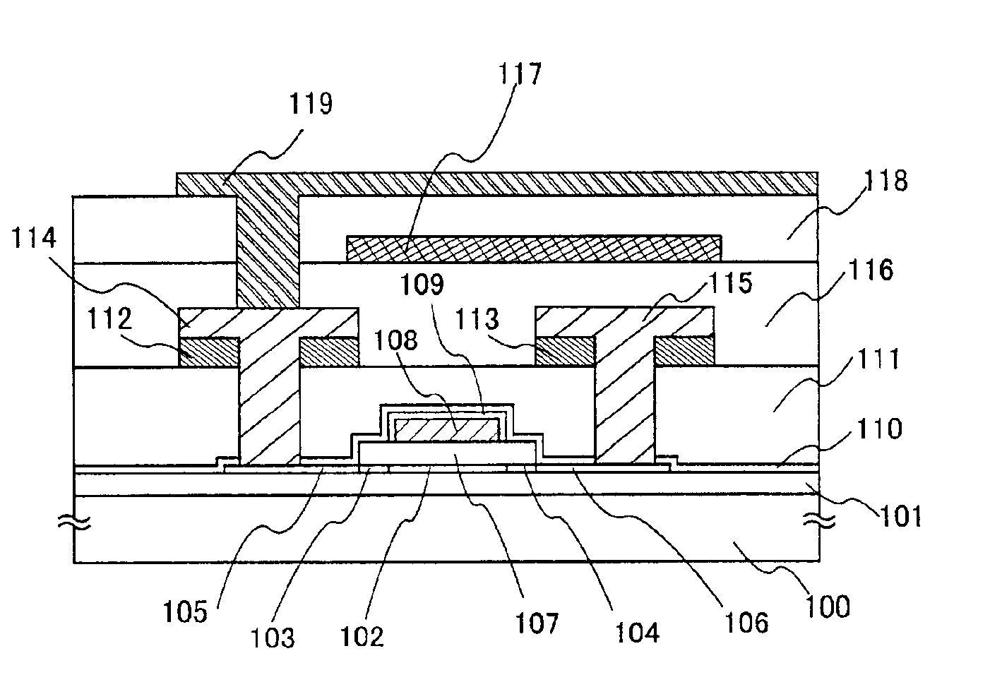
This embodiment is explained referring to FIG. 1, which shows a cross-sectional structure of a semiconductor element of the present invention, fabricated on an insulating substrate.

Referring to the drawing, reference number 100 denotes a substrate and 101 denotes an underlying film. In addition, reference number 102 denotes a channel forming region, 103 and 104 denote low concentration impurity regions, 105 denotes a drain region, 106 a source region, 107 a gate insulating film, 108 a gate wiring, 109 an anode oxide film, and 110 a passivation film. Moreover, reference number 111 denotes an organic material film (a first inter-layer insulating film), 112 and 113 denote first metallic layers, 114 and 115 second metallic layers, 116 denotes an organic material film (a second inter-layer insulating film), and 117 a black mask. Still moreover, reference number 118 denotes an organic material film (a third inter-layer insulating film) and 119 a pixel electrode.

The wirings (112 to 115) ha...

embodiment 2

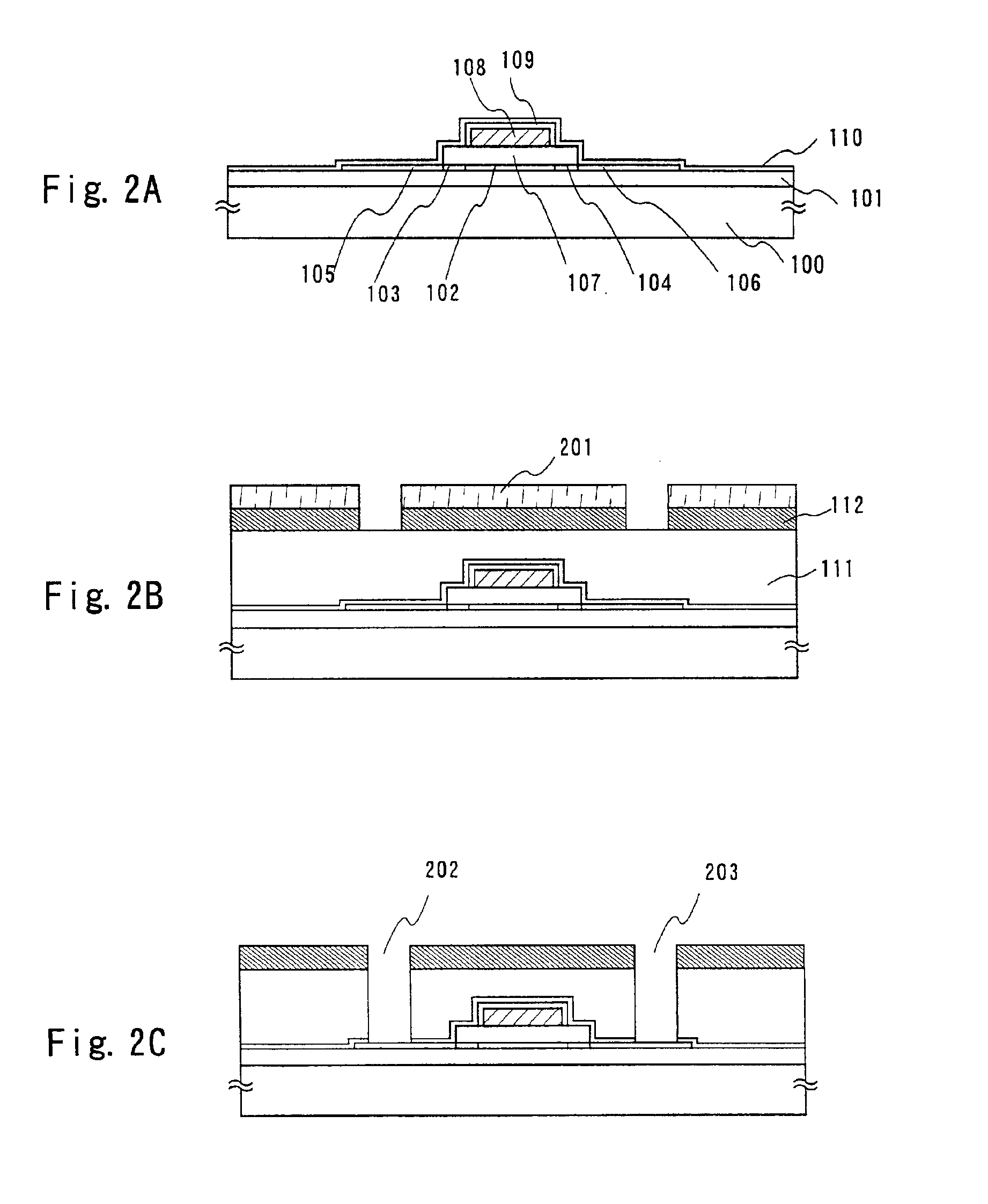
In this embodiment, a process for fabricating a semiconductor element, in particular, a process for forming contact holes and wirings, on a substrate having insulating surfaces, is explained below with reference to FIG. 2 and FIG. 3.

First, the underlying film 101 is formed on the substrate 100 having insulating surfaces. A glass substrate, a quartz substrate, a ceramic substrate, or a semiconductor substrate can be used as the substrate. A glass substrate was used in this embodiment. The underlying film can employ a silicon oxide film, a silicon nitride film, or a silicon oxinitride film, 100 to 300 nm in thickness of the film. This embodiment employs TEOS as a raw material to form a silicon oxide film 200 nm in thickness. Furthermore, if sufficient flatness is available such as a quartz substrate, no underlying film need be necessarily provided.

Next, an active layer is formed on the substrate or the underlying film. The active layer may be made up of a crystalline semiconductor fil...

embodiment 3

This embodiment is an example of employing an inversely staggered TFT, the structure of which is shown in FIG. 4. The processes of this embodiment, which are different from those for fabricating inversely staggered TFTs by means of a known technique, are as follows. That is, the process in which an organic material is used for an inter-layer insulating film 411, the process in which contact holes are formed by dry etching using a metallic film as a mask, and the process in which wirings are formed which are constituted by a first metallic film 412 and a second metallic film 414. Furthermore, the structure of the TFT is not limited to the configuration (a channel stop type) shown in FIG. 4. The present invention can be readily applied even to such a structure, for example, as has a channel etch TFT or a silicide structure.


PUM

PropertyMeasurementUnit
diameteraaaaaaaaaa
thicknessaaaaaaaaaa
thicknessaaaaaaaaaa

Abstract

The object is to pattern extremely fine integrated circuits by forming fine contact holes. The dry etching method is employed to form contact holes to pattern a wiring (114), using a mask made of metallic film (112) and an organic material as an inter-layer insulating film (111) for covering switching elements and each of the wirings.

Description

FIELD OF THE INVENTIONThe present invention relates to a structure and the method for fabricating a semiconductor device. More particularly, it relates to an active matrix liquid-crystal display device which employs semiconductor thin layer and a method for fabricating the device. Moreover, the present invention can be applied to electro-optical devices comprising such a display device.Furthermore, it is to be understood that any device that can function by employing semiconductor properties is called a semiconductor device in this specification. Accordingly, the semiconductor devices cited in the aforementioned claims include not only single semiconductor elements such as TFTs but also semiconductor circuits comprising semiconductor elements, electro-optical devices, and electrical apparatuses to which these are mounted as components. A thin film transistor (TFT) is a representative example of semiconductor elements. Also available are an insulating-gate field effect transistor (IG...

Claims


Application Information

Patent Timeline
Patent Type & Authority Patents(United States)
IPC IPC(8): G02F1/13G02F1/1362H01L21/70H01L29/786H01L29/66H01L21/768H01L21/84H01L21/77H01L27/13
CPCG02F1/136227H01L21/76802H01L21/76838H01L21/76885H01L29/78636H01L27/1255H01L27/124H01L27/1248H01L29/41733H01L29/458H01L2924/0002H01L2924/00
Inventor OHTANI, HISASHINAKAZAWA, MISAKOMURAKAMI, SATOSHIFUJIMOTO, ETSUKO
Owner SEMICON ENERGY LAB CO LTD
Why Eureka
Try Eureka