System and method for detection of electromagnetic radiation by amorphous silicon x-ray detector for metal detection in x-ray imaging

a technology of amorphous silicon and detector, which is applied in the field of detection of electromagnetic radiation by an amorphous silicon x-ray detector for metal detection in x-ray imaging, can solve the problems of reducing the value of the image to the medical practitioner, streak artifacts, and artifacts in the image, so as to improve the image quality and improve the image quality

Inactive Publication Date: 2010-05-04
GENRERAL ELECTRIC CO
View PDF24 Cites 122 Cited by
  • Summary
  • Abstract
  • Description
  • Claims
  • Application Information

AI Technical Summary

Benefits of technology

[0015]Certain embodiments of the present invention provide a method for improving image quality in an imaging system including emitting an electromagnetic field with an electromagnetic transmitter, reading a first field image from an imaging system detector based at least in part on the electromagnetic field, positioning an object to be imaged by the imaging system, reading a second field image from the detector based at least in part on the electromagnetic field, and detecting the presence of metal based at least in part on at least one of the first field image and the second field image. In an embodiment, the detector is a flat panel detector, such as an amorphous silicon flat panel x-ray detector. In an embodiment, the image is an x-ray image. In an embodiment, the electromagnetic transmitter is used in a surgical navigation system. In certain embodiments, the method further includes reading an object image from the detector and processing the object image with a metal artifact reduction algorithm when metal is detected. In an embodiment, the object image is an x-ray image.
[0016]Certain embodiments of the present invention provide an apparatus for improving image quality in an imagine system that includes an imaging system detector and an image processing component. The detector is capable of acquiring a first field image, a second field image, and an object image. The image processing component is in communication with the detector. The image processing component adjusts the object image based at least in part on the first and / or second field images. In an embodiment, the detector is a flat panel detector, such as an amorphous silicon flat panel x-ray detector. In an embodiment, the object image is an x-ray image. In an embodiment, at least one of the first and second field images is based at least in part on an electromagnetic field sensed by the detector. In an embodiment, the electromagnetic field is emitted at least in part by a surgical navigation device. In an embodiment, the first field image differs from the second field image based at least in part on the presence of metal in an object being imaged by the imaging system. In certain embodiments, the image processing component utilizes a metal artifact reduction algorithm to process the object image when metal is sensed by the detector. In an embodiment, the first field image is acquired when no object is positioned to be imaged by the imaging system. In an embodiment, the second field image is acquired when an object is positioned to be imaged by the imaging system.

Problems solved by technology

However, metal or other materials capable of distorting electromagnetic fields in the object being imaged can result in artifacts or distortions in the image.
For example, metal in the area of the patient being x-rayed, such as pedicle screws in the spine, can cause streak artifacts.
These distortions or artifacts may generally reduce the value of the image to the medical practitioner.
This amplification occurs in part because there is less data available in the 2D images, due to the artifacts and distortions, to properly assemble the voxels for the 3D image.
Another potential source of artifacts or distortions in images are electromagnetic fields.
One or more parts of the detector of the imaging system may be susceptible to electromagnetic fields.
The electromagnetic field may result in distortions or artifacts in the images read from the detector in part because the electromagnetic fields introduce spurious signals or noise into one or more of the components of the detector.
This noise may appear as artifacts or distortions in the images read from the detector.

Method used


Image

  • System and method for detection of electromagnetic radiation by amorphous silicon x-ray detector for metal detection in x-ray imaging
  • System and method for detection of electromagnetic radiation by amorphous silicon x-ray detector for metal detection in x-ray imaging
  • System and method for detection of electromagnetic radiation by amorphous silicon x-ray detector for metal detection in x-ray imaging

Examples


Embodiment Construction

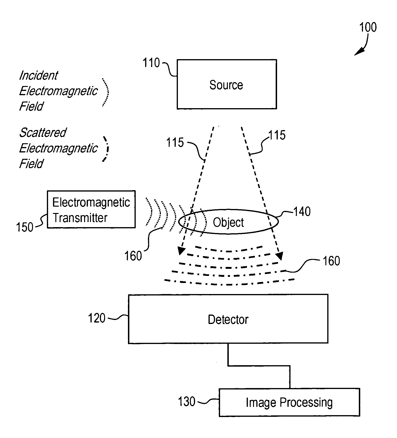
[0024]FIG. 1 illustrates an imaging system 100 used in accordance with an embodiment of the present invention. For the purposes of illustration, the imaging system 100 is described as an x-ray system. The imaging system 100 includes subsystems such as an x-ray source 110, an x-ray detector 120, and an image processing component 130. Also, an object 140 to be imaged may be present. The imaging system 100 may also include an electronic transmitter 150.

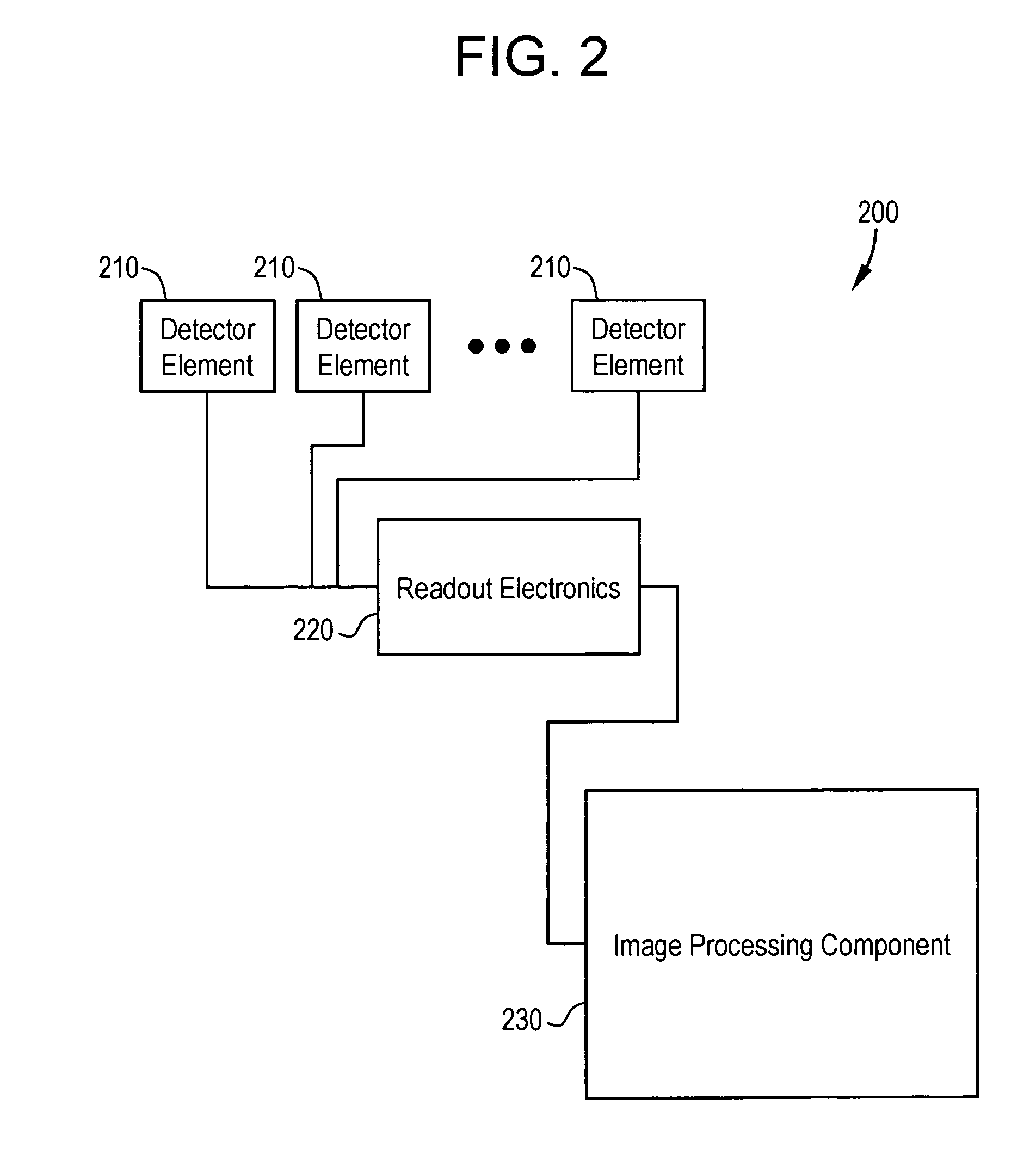
[0025]The detector 120 may be, for example, a flat panel detector, such as an amorphous silicon flat panel x-ray detector. The detector 120 may include and / or be connected to an array of detector elements and readout electronics. The readout electronics may be part of a data acquisition component. The readout electronics are in communication with the detector elements. The components of the detector 120 may be connected by wires and / or conductors, for example. The detector 120 may be sensitive to and / or affected by electromagnetic signal...


PUM


Abstract

Certain embodiments of the present invention provide a method for detecting an electromagnetic field in an imaging system including emitting an electromagnetic field with an electromagnetic transmitter, sensing an electromagnetic field with an imaging system detector, and reading a field image from the detector based at least in part on the electromagnetic field. The imaging system detector is capable of reading an object image and a field image. The detector may be an amorphous silicon flat panel x-ray detector. The electromagnetic transmitter may be used in surgical navigation. The position of a surgical device, instrument, and / or tool may be determined based in part on the field image. The detector may be coordinated to acquire the field image when the electromagnetic transmitter is emitting an electromagnetic field. The detector may be coordinated to acquire the object image when the electromagnetic transmitter is not emitting an electromagnetic field.

Description

BACKGROUND OF THE INVENTION[0001]The present invention generally relates to amorphous silicon x-ray detectors. In particular, the present invention relates to the detection of electromagnetic radiation by an amorphous silicon x-ray detector for metal detection in x-ray imaging.[0002]Digital imaging systems may be used to capture images to assist a physician in making an accurate diagnosis. Digital radiography imaging systems typically include a source and a detector. Energy, such as x-rays, produced by the source travel through an object to be imaged and are detected by the detector. An associated image processing system obtains image data from the detector and prepares a corresponding diagnostic image on a display.[0003]The detector may be an amorphous silicon flat panel detector, for example. Amorphous silicon is a type of silicon that is not crystalline in structure. Image pixels are formed from amorphous silicon photodiodes connected to switches on the flat panel. A scintillator...

Claims


Application Information

Patent Timeline
Patent Type & Authority Patents(United States)
IPC IPC(8): A61B5/05
CPCA61B5/06G01N23/04A61B6/12A61B5/062
Inventor KUHN, PAUL KENNETHANDERSON, PETER TRANEUSLAMBERTY, JOHN ROBERT
Owner GENRERAL ELECTRIC CO
Why Eureka
Try Eureka