Semiconductor device with vertical channel transistor and method for fabricating the same

a technology of vertical channel transistor and semiconductor device, which is applied in the direction of semiconductor device, basic electric element, electrical apparatus, etc., can solve the problems of difficult to realize a high-speed memory device, and difficulty in downscaling memory devices having a line width of 40 nm or less, so as to reduce the total resistance of a word line and high-speed performance

Active Publication Date: 2010-05-11
SK HYNIX INC
View PDF12 Cites 29 Cited by
  • Summary
  • Abstract
  • Description
  • Claims
  • Application Information

AI Technical Summary

Benefits of technology

[0009]Embodiments of the present invention are directed to providing a semiconductor device including a vertical channel transistor that can realize high-speed performance by reducing a total resistance of a word line, and a method for fabricating the semiconductor device.

Problems solved by technology

However, it is very difficult to realize a downscaled memory device having a line width of 40 nm or less using a typical planar or recessed gate transistor having an 8F2 or 6F2 cell architecture (where ‘F’ represents a minimum feature size).
Therefore, a total sheet resistance (RS) of the word line 18 dramatically increases due to the small area of the gate electrode 14, making it difficult to realize a high-speed memory device.

Method used


Image

  • Semiconductor device with vertical channel transistor and method for fabricating the same
  • Semiconductor device with vertical channel transistor and method for fabricating the same
  • Semiconductor device with vertical channel transistor and method for fabricating the same

Examples


Embodiment Construction

[0018]Hereinafter, a semiconductor device including a vertical channel transistor and a method for fabricating a semiconductor device including a vertical channel transistor in accordance with the present invention are described in detail with reference to the accompanying drawings.

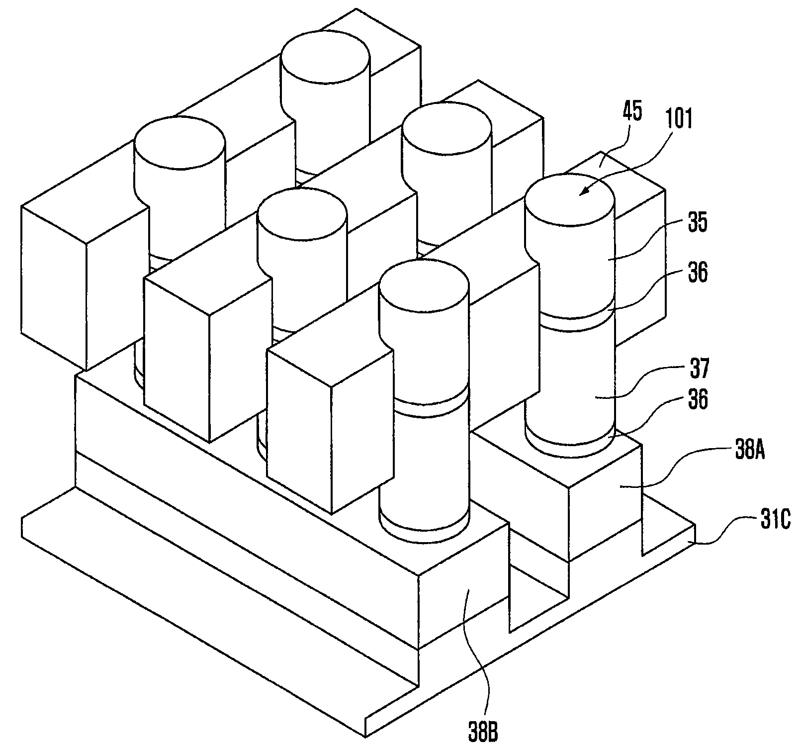
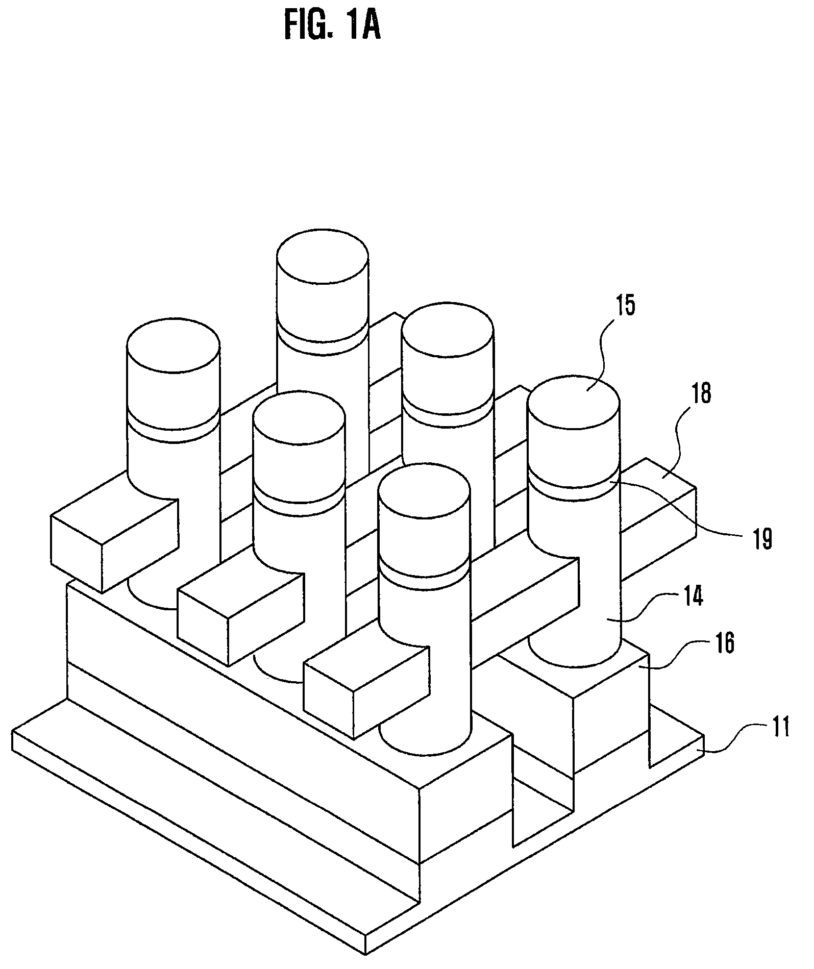
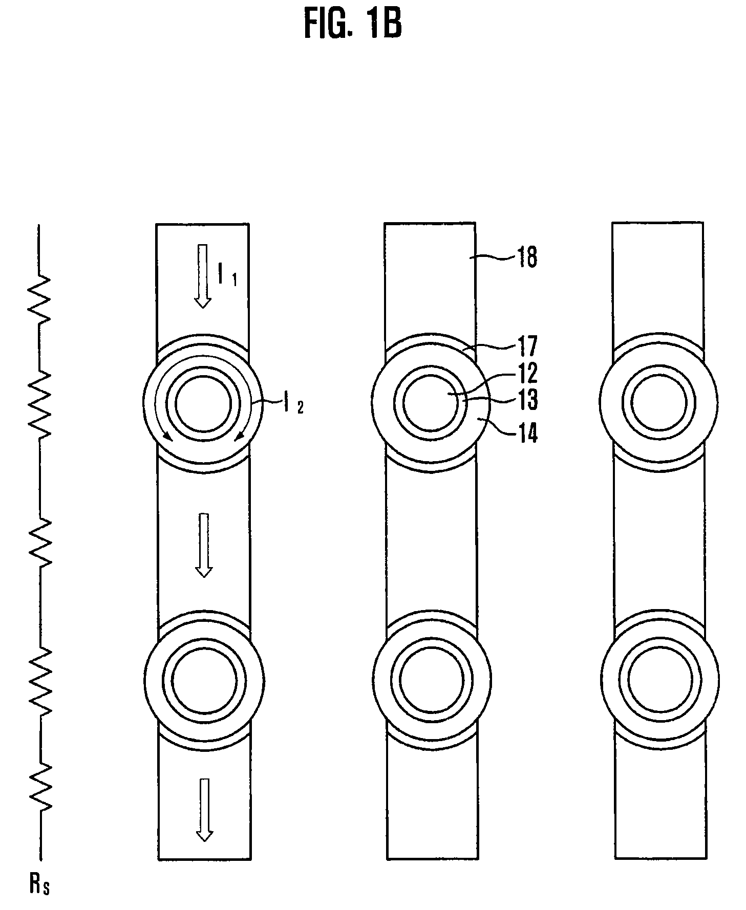
[0019]FIG. 2A illustrates a perspective view of a semiconductor device in accordance with an embodiment of the present invention. FIG. 2B illustrates a cross-sectional view of the semiconductor device in accordance with the embodiment of the present invention. FIG. 2C illustrates a plan view of a connection between a word line and a gate electrode in the semiconductor device in accordance with the embodiment of the present invention. For convenience, an insulation layer or the like is omitted from the drawings.

[0020]Referring to FIGS. 2A to 2C, a plurality of pillar structures 101 are formed over a substrate 31C in the form of a matrix, and are separated from each other by a predetermined distance. The pi...


PUM


Abstract

In a high speed vertical channel transistor, a pillar structure is formed over a substrate, a gate electrode surrounds an outer wall of a lower portion of the pillar structure; and a word line extends in a direction to partially contact an outer wall of the gate electrode. The word line shifts toward a side of the pillar structure resulting in increased transistor speed.

Description

CROSS-REFERENCE TO RELATED APPLICATIONS[0001]The present invention claims priority of Korean patent application number 10-2007-0111632, filed on Nov. 2, 2007, which is incorporated by reference in its entirety.BACKGROUND OF THE INVENTION[0002]The present invention relates to semiconductor device fabrication technology, and more particularly, to a semiconductor device with a vertical channel transistor and a method for fabricating a semiconductor device with a vertical channel transistor.[0003]Recently, there has been an increasing need for sub-40 nm memory devices to increase the degree of integration. However, it is very difficult to realize a downscaled memory device having a line width of 40 nm or less using a typical planar or recessed gate transistor having an 8F2 or 6F2 cell architecture (where ‘F’ represents a minimum feature size). Therefore, dynamic random access memory (DRAM) devices having 4F2 cell architectures are now required since they improve the degree of integratio...

Claims


Application Information

Patent Timeline
Patent Type & Authority Patents(United States)
IPC IPC(8): H01L21/8236
CPCH01L29/7827H01L29/66666H01L27/10891H01L27/10876H10B12/053H10B12/488H01L21/18
Inventor SUNG, MIN-GYUCHO, HEUNG-JAEKIM, YONG-SOOLIM, KWAN-YONGJANG, SE-AUG
Owner SK HYNIX INC
Why Eureka
Try Eureka