MOS transistor having double gate and manufacturing method thereof

Inactive Publication Date: 2007-05-31
DONGBU ELECTRONICS CO LTD
View PDF12 Cites 35 Cited by
  • Summary
  • Abstract
  • Description
  • Claims
  • Application Information

AI Technical Summary

Benefits of technology

[0011] An object of the present invention is to provide a MOS transistor with low power and high-speed performance b

Problems solved by technology

However, due to the region of the substrate for supporting the semiconductor device, which is referred to as the region for a support substrate in brief, an excessive power is consumed.
Moreover, due to a parasitic effect, e.g., t

Method used


Image

  • MOS transistor having double gate and manufacturing method thereof
  • MOS transistor having double gate and manufacturing method thereof
  • MOS transistor having double gate and manufacturing method thereof

Examples


Example

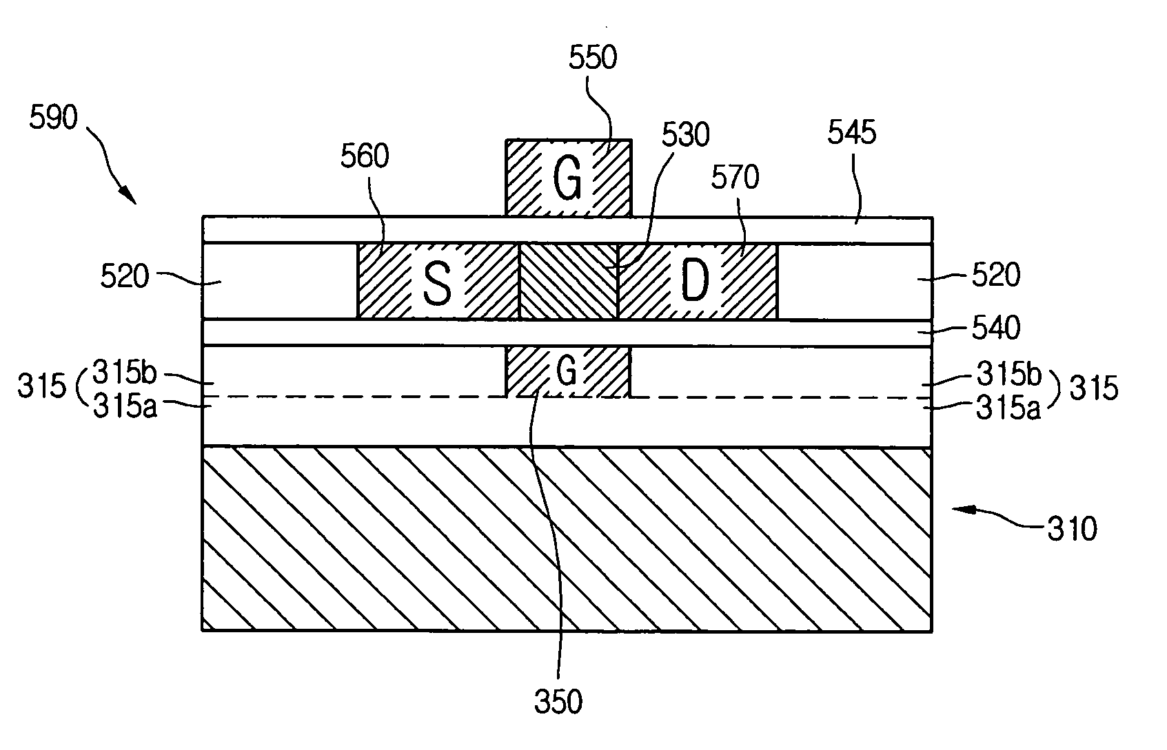
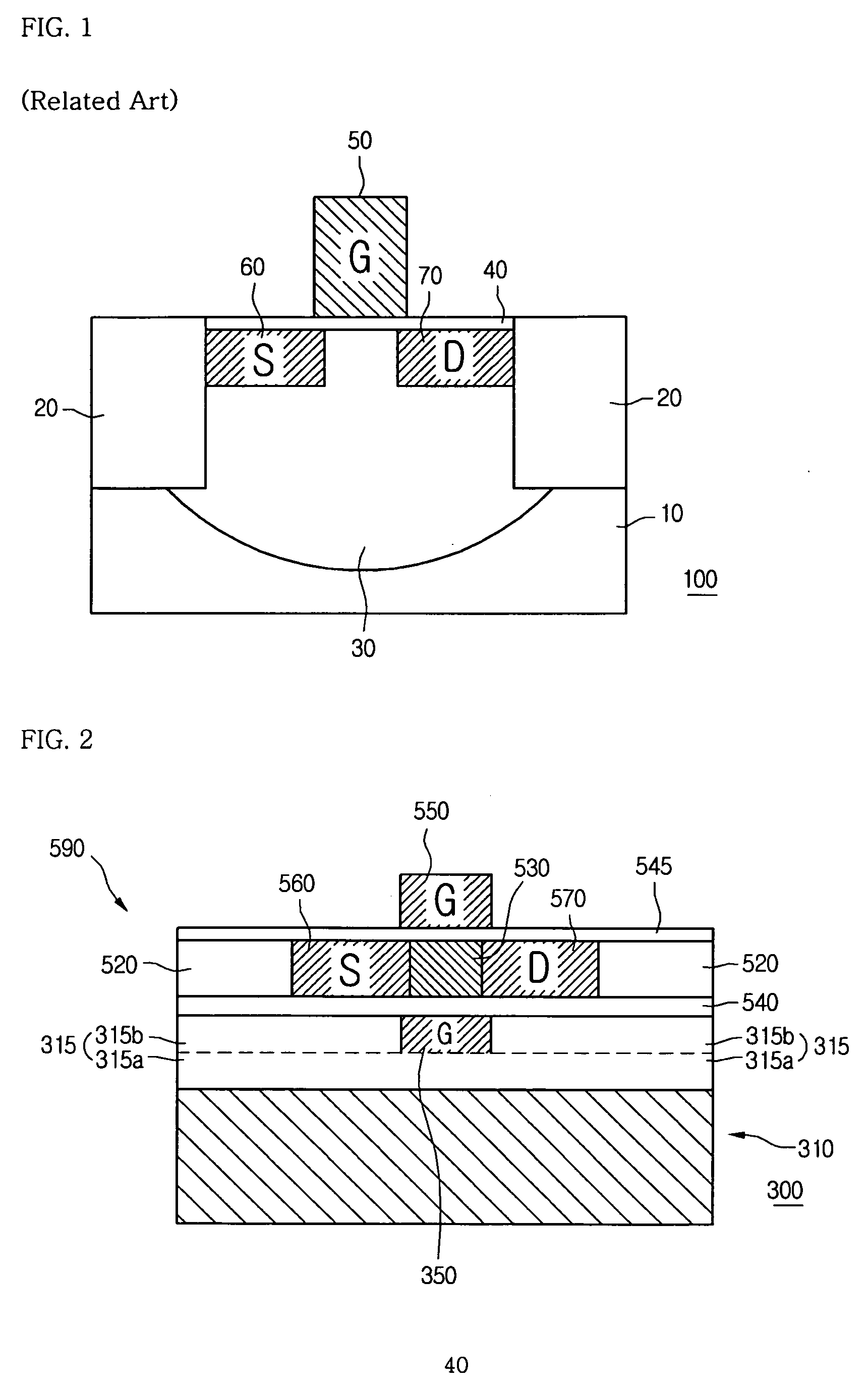
[0024]FIG. 2 is a cross-sectional view of a MOS transistor having a double gate according to a first embodiment of the present invention.

[0025] The MOS transistor 300 having the double gate according to the first embodiment of the present invention includes a substrate 310, a first gate 350, a first gate oxide layer 540, a silicon layer 590, a source region 560, a drain region 570, a second gate oxide layer 545, and a second gate 550. Herein, an insulating layer 315 is formed on the substrate 310. The first gate 350 is embedded in the insulating layer 315, wherein a top surface of the first gate 350 is exposed. The first gate oxide layer 540 is formed on the insulating layer 315 and the first gate 350. The silicon layer 590 is formed on the first gate oxide layer 540. The source and drain regions 560 and 570 are formed in the silicon layer 590 to be in contact with the first gate oxide layer 540. The second gate oxide layer 545 is formed on the silicon layer 590 such that it is in ...

Example

Second Embodiment

[0049] In a method of forming a MOS transistor having a double gate according to a second embodiment of the present invention, a gate oxide layer 540 is not formed on a silicon layer 590, unlike the first embodiment.

[0050] The method according to the second embodiment of the present invention includes: a) preparing a substrate, wherein a first gate is embedded in an upper portion of the substrate; b) preparing a silicon layer; c) bonding the top surface of the substrate and the top surface of the silicon layer together; d) forming the source region and the drain region to be in contact with the first gate oxide layer by implanting an impurity into the silicon layer on both sides of the gate; e) forming the second gate oxide layer on the silicon layer to be in contact with the source and drain regions; f) forming the second gate on the second gate oxide layer disposed between the source region and the drain region.

[0051] During the process of bonding the top surfa...

Example

Third Embodiment

[0052] In a method of forming a MOS transistor having a double gate according to a third embodiment of the present invention, an oxide layer is formed on a substrate in which a gate is embedded in an upper portion thereof, unlike the first embodiment.

[0053] The method according to the third embodiment of the present invention includes: a) preparing a substrate having a first gate oxide layer formed thereon, wherein a first gate is embedded in an upper portion of the substrate; b) preparing a silicon layer; c) bonding the top surface of the substrate and the top surface of the silicon layer together; d) forming the source region and the drain region to be in contact with the first gate oxide layer by implanting an impurity into the silicon layer on both sides of the gate; e) forming the second gate oxide layer on the silicon layer to be in contact with the source and drain regions; f) forming the second gate on the second gate oxide layer disposed between the source...


PUM


Abstract

There are provided a MOS transistor having a double gate and a manufacturing method thereof. The MOS transistor includes a substrate on which an insulating layer is formed, a first gate embedded in the insulating layer, in which the top surface of the first gate is exposed, a first gate oxide layer formed on the insulating layer and the first gate, a silicon layer formed on the first gate oxide layer, a source region and a drain region formed in the silicon layer to be in contact with the first gate oxide layer, a second gate oxide layer formed on the silicon layer to be in contact with the source and drain regions, and a second gate formed on the second gate oxide layer disposed between the source region and the drain region.

Description

BACKGROUND OF THE INVENTION [0001] 1. Field of the Invention [0002] The present invention relates to a semiconductor device, and more particularly, to a metal oxide semiconductor (MOS) transistor and a manufacturing method thereof. [0003] 2. Description of the Related Art [0004] A related art metal oxide semiconductor (MOS) transistor will be described with reference to FIG. 1. [0005]FIG. 1 is a cross-sectional view of a related art MOS transistor 100. [0006] In general, according to a process of forming an NMOS transistor, an oxide such as a shallow trench isolation (STI) 20 is formed in a p-type substrate 10 to isolate a device from each other, and then an impurity is implanted so as to form a well 30. A thin gate oxide layer 40 is formed on the substrate 10 in which the well 30 is formed. Thereafter, polysilicon is deposited on the resultant structure, and then is etched to form a gate 50. Thereafter, an impurity is implanted again into the substrate 10 on both sides of the gate ...

Claims


Application Information

Patent Timeline
IPC IPC(8): H01L29/76
CPCH01L29/66772H01L29/78648H01L21/18
Inventor YUN, HYUNG SUN
Owner DONGBU ELECTRONICS CO LTD
Why Eureka
Try Eureka