CMOS compatible low band offset double barrier resonant tunneling diode

a tunneling diode and low band offset technology, applied in the field of solid-state electronics, can solve the problems of difficult integration of rtds into mainstream si cmos ic technology, siosub>2/sub>/si type rtds, and difficult to achieve high peak-to-valley ratio and good i-v characteristics

Inactive Publication Date: 2005-03-17
AGENCY FOR SCI TECH & RES +1
View PDF9 Cites 94 Cited by
  • Summary
  • Abstract
  • Description
  • Claims
  • Application Information

AI Technical Summary

Benefits of technology

[0010] A second object of the present invention is to provide a method of forming such a device wherein good I-V characteristics, such as high peak-to-valley ratio (PVR), are obtained.

Problems solved by technology

However, RTDs have been difficult to integrate into mainstream Si CMOS IC technology.
SiO2 is not the only material suitable for the barrier layer that has a wider band gap than silicon.
Although the SiO2 double barrier structure with a silicon well was reported in H. Ikeda, M. Iwasaki, Y. Ishikawa, and M. Tabe, “Resonant tunneling characteristics in SiO2 / Si double barrier structure in a wide range of applied voltage,” Applied Physics Letters, vol.83, pp.1456-1458, 2003, it remains a challenge for SiO2 / Si type RTDs to find their way into applications due to poor performance which is due mainly to the large band offset between SiO2 and Si and the excessive thickness SiO2 of the buried oxide layer in a silicon-on-insulator (SOI) substrate.
Okuno, in both (U.S. Pat. No. 5,466,949) and (U.S. Pat. No. 5,616,515) discloses a resonant tunneling diode formed by layering silicon dioxide barrier layers on either side of a germanium well, but, as already noted, this device structure is not compatible with silicon processing schemes.
The fabrication of such a device would not fit smoothly within the convention silicon process flow scheme.

Method used


Image

  • CMOS compatible low band offset double barrier resonant tunneling diode
  • CMOS compatible low band offset double barrier resonant tunneling diode
  • CMOS compatible low band offset double barrier resonant tunneling diode

Examples


Embodiment Construction

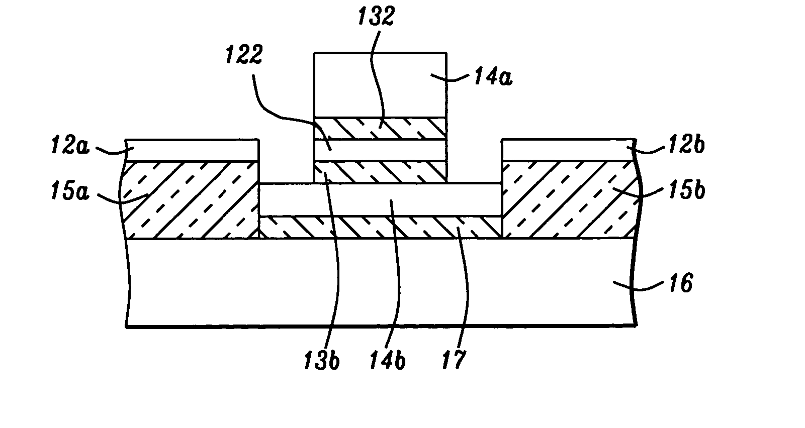
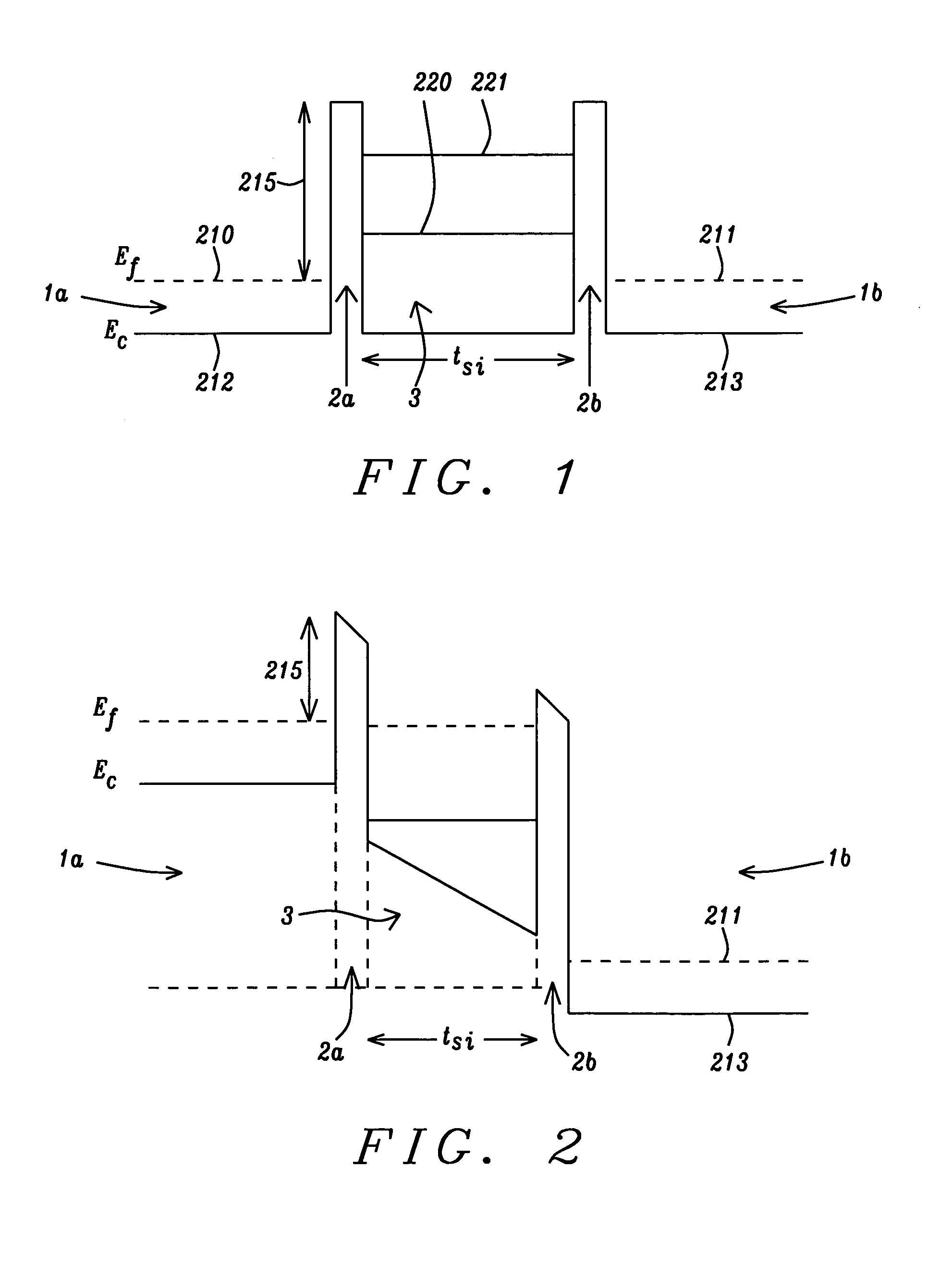
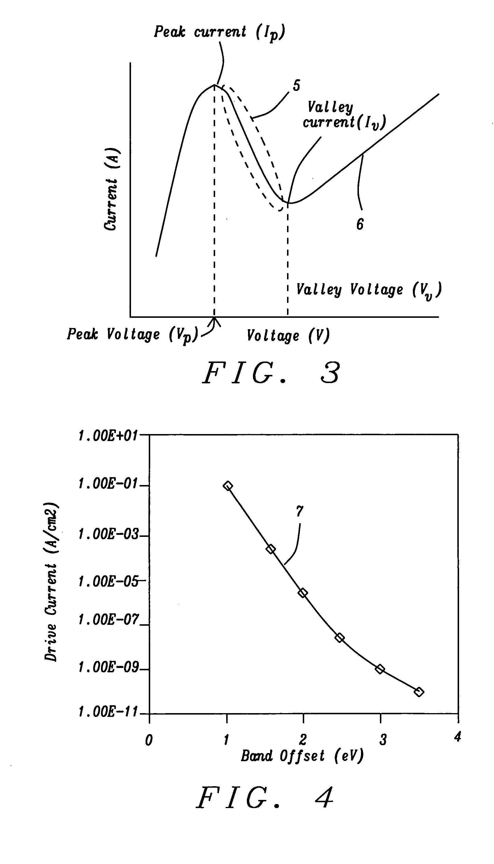
[0024] The preferred embodiments of the present invention include three methods of forming a RTD structure using low band offset dielectrics as barrier layers formed adjacent to and in contact with a quantum well formed of a silicon layer. In the case of the silicon layer, the fabrication process will begin most advantageously with a silicon-on oxide (SOI) substrate, which is a substrate of choice in many fabrication processes. However, the method to be presented can also be applied advantageously to Ge quantum wells and to SiGe quantum wells, in which cases the substrate of choice would be a Ge-on-oxide (GOI) substrate or a SiGe-on-oxide substrate. It is also envisioned that other semiconductor materials could be formed into quantum well structures, in which case other substrates could be employed. Although the examples to be presented specifically mention Si, Ge and SiGe and although Si is most probbly the most common semiconductor material being employed in semiconductor fabricat...


PUM


Abstract

Three configurations of double barrier resonant tunneling diodes (RTD) are provided along with methods of their fabrication. The tunneling barrier layers of the diode are formed of low band offset dielectric materials and produce a diode with good I-V characteristics including negative differential resistance (NDR) with good peak-to-valley ratios (PVR). Fabrication methods of the RTD start with silicon-on-insulator substrates (SOI), producing silicon quantum wells, and are, therefore, compatible with main stream CMOS technologies such as those applied to SOI double gate transistor fabrication. Alternatively, Ge-on-insulator or SiGe-on-insulator substrates can be used if the quantum well is to be formed of Ge or SiGe. The fabrication methods include the formation of both vertical and horizontal silicon quantum well layers. The vertically formed layer may be oriented so that its vertical sides are in any preferred crystallographic plane, such as the 100 or 110 planes.

Description

[0001] This application claims priority to U.S. Provisional Application No. 60 / 503,110, filed on Sep. 15, 2003 and which is fully incorporated herein by reference.BACKGROUND OF THE INVENTION [0002] 1. Field of the Invention [0003] This invention relates to solid state electronics, in particular to a novel high frequency silicon based resonant tunnel diode with negative differential resistance. [0004] 2. Description of the Related Art [0005] The tunnel diode formed by a heavily doped p-n junction was invented by Esaki in 1958. This diode operated on the basis of interband tunneling, wherein charge carriers moved between valence and conduction bands by tunneling through an intervening potential barrier. Subsequently, in 1974, Esaki and co-workers demonstrated a resonant tunneling diode (RTD) consisting of two potential barriers separated by a potential well using a III-V compound semiconductor (L. L Chang, L. Esaki, and R. Tsu, “Resonant tunneling in the semiconductor double barriers,...

Claims


Application Information

Patent Timeline
Patent Type & Authority Applications(United States)
IPC IPC(8): G11C5/14H01L27/06H01L29/88
CPCB82Y10/00G11C5/142H01L29/882H01L29/785H01L27/0629
Inventor LI, MING FUSINGH, JAGARHOU, YONG TIANBALASUBRAMANIAN, NARAYANANLIN, FUJIANG
Owner AGENCY FOR SCI TECH & RES
Why Eureka
Try Eureka