Nonvolatile semiconductor memory device

a semiconductor memory and non-volatile technology, applied in the direction of water treatment parameter control, instruments, transportation and packaging, etc., can solve the problem of small operation margin at the time of readout, and achieve the effect of high speed

Inactive Publication Date: 2006-03-28
SHARP KK
View PDF3 Cites 37 Cited by
  • Summary
  • Abstract
  • Description
  • Claims
  • Application Information

AI Technical Summary

Benefits of technology

[0024]The present invention was made in view of the above problems and it is an object of the present invention to provide a semiconductor memory device in which the problems regarding the trimming of the reference memory cell are solved and multi-level cells can be handled and a readout operation can be performed stably at high speed.
[0027]According to the nonvolatile semiconductor memory device comprising the first characteristics of the present invention, since the readout circuit commonly uses the reference memory cell set in the same storage state at the time of the normal readout and at the time of the readout for the program verification (at the time of the verification), the number of the reference memory cells can be reduced. In addition, since the substantial threshold voltage difference between at the time of the normal readout and at the time of the verification is implemented by a difference of the electric stresses applied to the reference memory cell at the time of the verification, the error at the time of setting the threshold voltage of the reference memory cell appears equally at the time of the normal readout and at the time of the verification, so that the threshold voltage difference being narrowed by the error at the time of setting the threshold voltage and readout margin being lowered do not occur. As a result, a nonvolatile semiconductor memory device which can deal with the multi-level cells and perform the readout operation stably at high speed can be provided.
[0030]Furthermore, according to the nonvolatile semiconductor memory device comprising the second characteristics of the present invention, the variation in voltage level applied to the gate of the nonvolatile memory transistor of each of the programmed memory cell and the reference memory cell at the time of the program verification appears in the same direction because it is based on the same internal voltage. Therefore, the variation in the threshold voltage because of the voltage variation in the gate of the reference memory cell is offset by the similar variation in the threshold voltage of the programmed memory cell; it is ensured that the threshold voltage of the programmed memory cell can be accurately compared with that of the reference memory cell. In addition, since the internal voltage level can be adjusted by the threshold voltage of the nonvolatile memory transistor, the variation in internal voltage level because of the manufacturing fluctuation can be compensated and the threshold voltage difference can be provided with high precision in many reference memory cells commonly by less number of adjustments.

Problems solved by technology

If such shifts occur, there is a problem such that the operation margin at the time of the readout becomes small.
In addition, the following problems are generated when the threshold voltage of the reference memory cell is set (referred to as “trimming”) at the time of the test in the conventional nonvolatile semiconductor memory device.

Method used


Image

  • Nonvolatile semiconductor memory device
  • Nonvolatile semiconductor memory device
  • Nonvolatile semiconductor memory device

Examples


Embodiment Construction

[0042]A nonvolatile semiconductor memory device according to one embodiment of the present invention (referred to as the “device of the present invention” occasionally hereinafter) will be described with reference to the accompanying drawings.

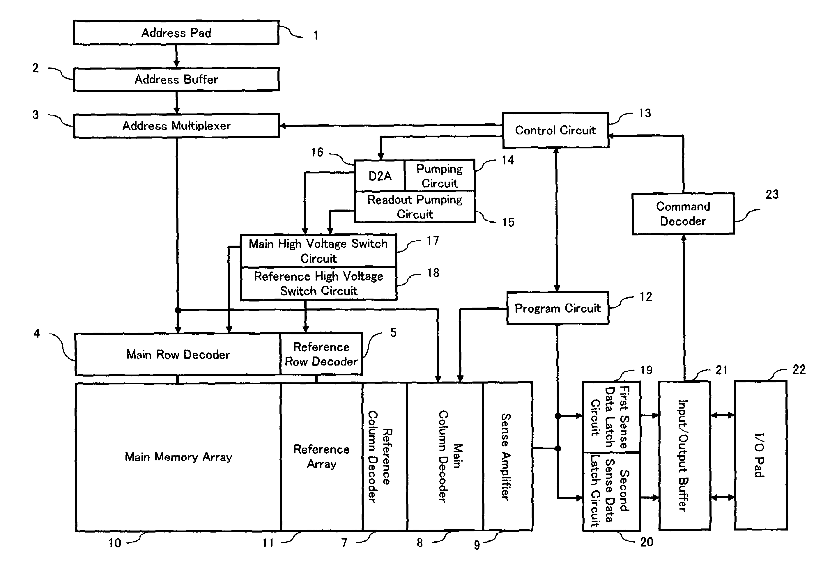
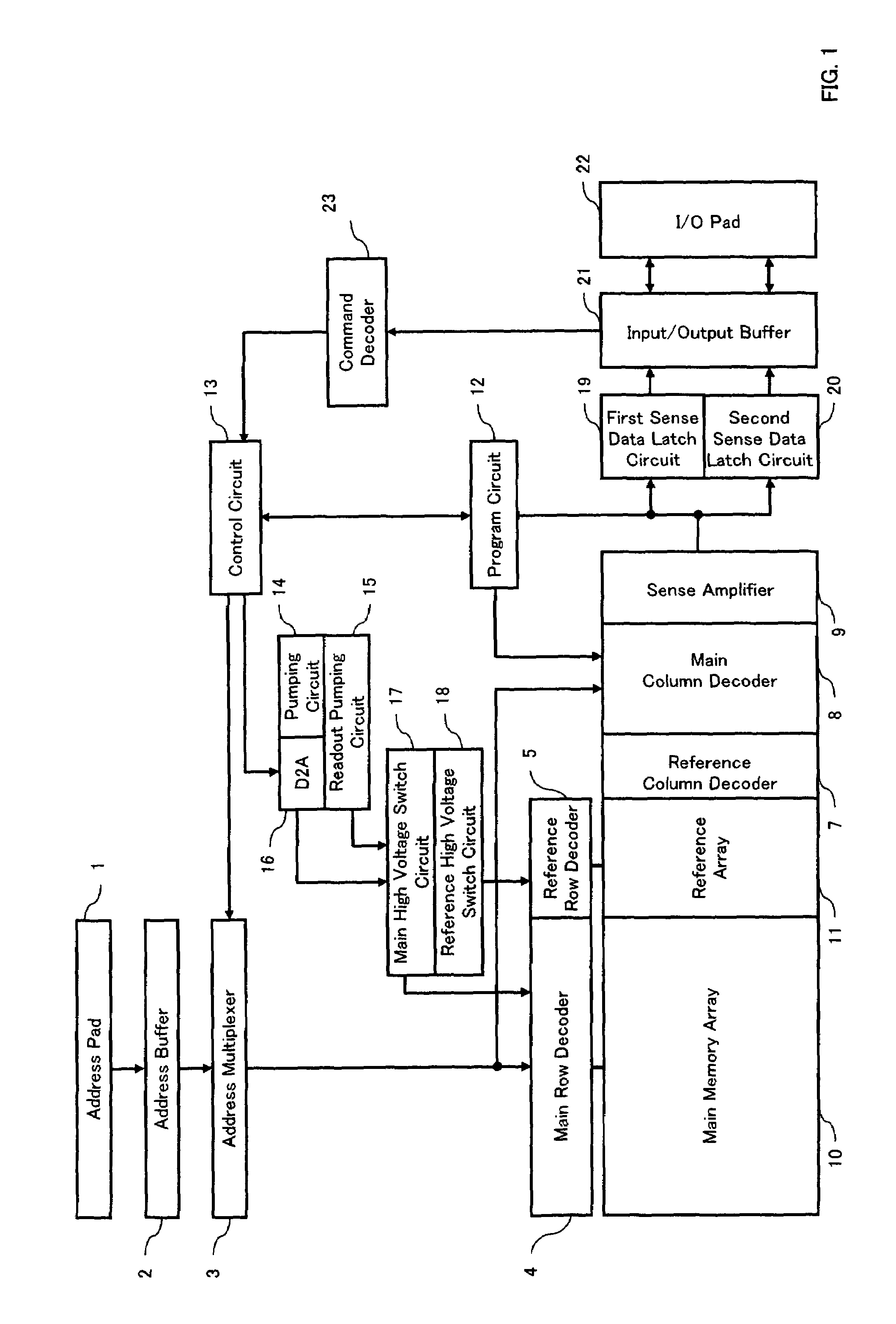
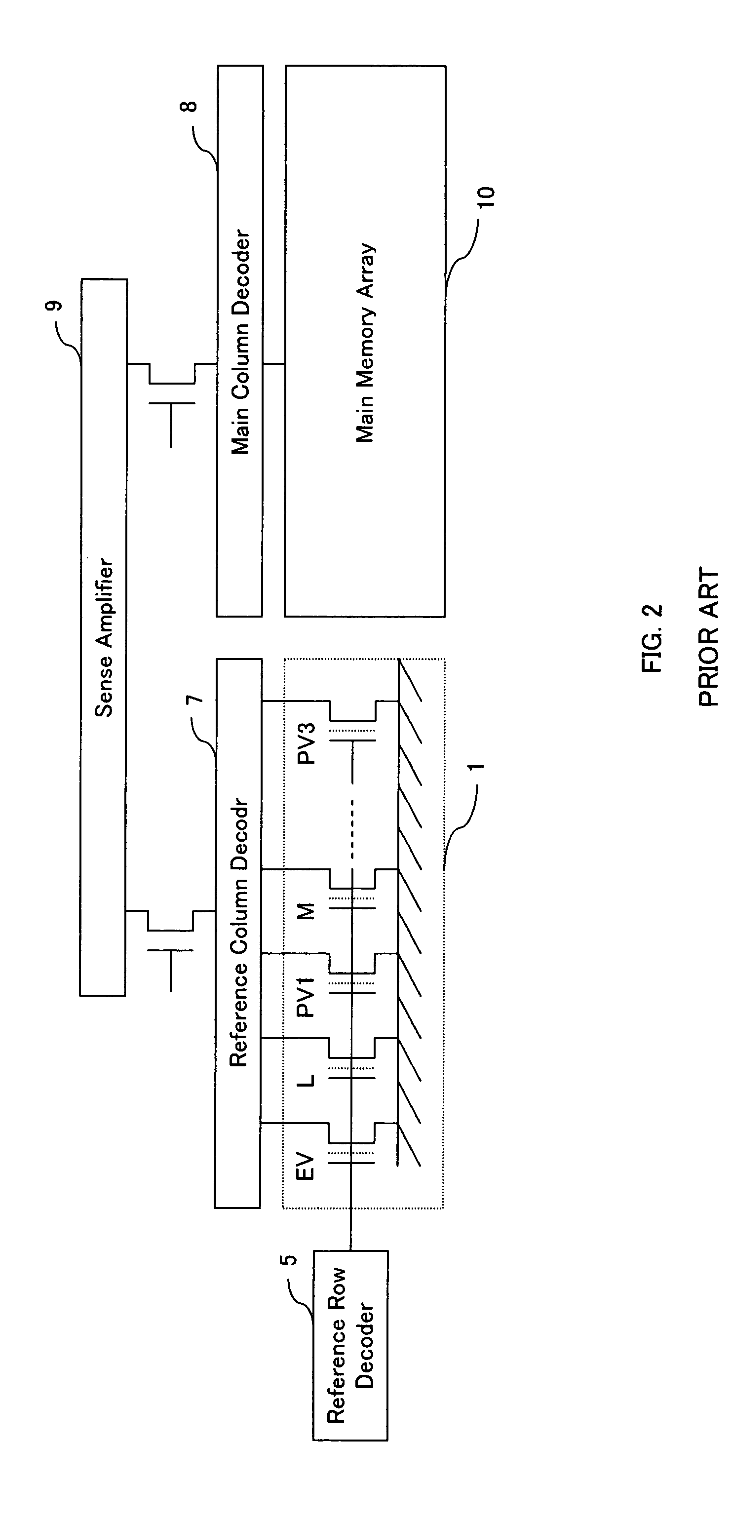
[0043]According to the device of the present invention, its functional block in the entire device is the same as that of a conventional flash memory in general, which is shown in FIG. 1.

[0044]Referring to FIG. 1, the device of the present invention comprises an address pad 1, an address buffer 2, an address multiplexer 3, a main row decoder 4, a reference row decoder 5, a reference column decoder 7, a main column decoder 8, a sense amplifier 9, a main memory array 10, a reference array 11, a program circuit 12, a control circuit 13, a pumping circuit 14, a readout pumping circuit 15, a digital / analog converter circuit (D2A) 16, a main high-voltage switch circuit 17, a reference high-voltage switch circuit 18, a first sense data latch circuit 19...


PUM

PropertyMeasurementUnit
threshold voltageaaaaaaaaaa
voltageaaaaaaaaaa
voltagesaaaaaaaaaa

Abstract

A nonvolatile semiconductor memory device includes a readout circuit which reads data stored in a selected memory cell by applying predetermined voltage to the selected memory cell and a reference cell such that currents corresponding to the respective threshold voltage may flow, and comparing the current flowing in the selected memory cell with the current flowing in the reference cell. The readout circuit commonly uses the reference cell set in the same storage state for normal readout and for readout for program verification, and when the predetermined voltage is applied to the selected memory cell and the reference memory cell at the time of the readout for the program verification, it sets an applying condition to the reference memory cell such that its storage state may be shifted more in the program state direction than that in an applying condition at the time of the normal readout.

Description

CROSS REFERENCE TO RELATED APPLICATTION[0001]This Nonprovisional application claims priority under 35 U.S.C. §119(a) on Patent Application No. 2004-030070 filed in Japan on Feb. 6, 2004, the entire contents of which are hereby incorporated by reference.BACKGROUND OF THE INVENTION[0002]1. Field of the Invention[0003]The present invention relates to a nonvolatile semiconductor memory device such as a flash memory and more particularly, it relates to a constitution of a reference cell which is a reference at the time of readout, or at the time of verification for program or erase of a memory cell of the nonvolatile semiconductor memory device.[0004]2. Description of the Related Art[0005]Various kinds of methods are employed in order to read a storage state of a memory cell in a semiconductor memory device. A description will be made of a flash memory which is one of the nonvolatile semiconductor memory devices as one example. The flash memory is constituted such that each memory cell c...

Claims


Application Information

Patent Timeline
Patent Type & Authority Patents(United States)
IPC IPC(8): G11C7/02G11C11/56G11C16/02G11C13/00G11C16/06G11C16/28G11C16/34
CPCG11C11/5642G11C11/5678G11C11/5685G11C13/0004G11C13/0007G11C13/0064G11C16/28G11C16/3436G11C13/004G11C2213/31G11C2013/0054B03D1/1431C02F1/24B01D21/0027C02F2209/02C02F2209/42B01F23/231
Inventor ANZAI, SHINSUKEMORI, YASUMICHI
Owner SHARP KK
Why Eureka
Try Eureka