Memory detecting circuit

a memory detection and circuit technology, applied in the field of detection circuits, can solve the problems of cpu with nothing to process, cpu with a bus speed greater than the ram speed, and costing a lot of time to arrange memories

Inactive Publication Date: 2010-05-11
HONG FU JIN PRECISION IND (SHENZHEN) CO LTD +1
View PDF3 Cites 0 Cited by
  • Summary
  • Abstract
  • Description
  • Claims
  • Application Information

AI Technical Summary

Benefits of technology

[0004]In a computer system, a central processing unit (CPU) reads data faster than a random access memory (RAM) can deliver, and usually the CPU has to wait for the RAM to deliver data. When the RAM is unable to keep up with the CPU, however, a bottleneck occurs, leaving the CPU with nothing to process. Under a single channel mode, any CPU with a bus speed greater than the RAM speed would be susceptible to the bottleneck effect. A dual channel mode is a technique used to alleviate the problem by doubling the amount of the available memory bandwidth. Instead of the single channel mode, a second parallel channel is added in the dual channel mode. With two channels working simultaneously, the bottleneck effect is reduced. Rather than waiting for the memory technology to improve, the dual channel mode simply takes the existing memory technology and modifies the method in which it is handled. With two channels working simultaneously, more information can be retrieved from the memory in the same amount of time, and thus improving the computer system performance.

Problems solved by technology

When the RAM is unable to keep up with the CPU, however, a bottleneck occurs, leaving the CPU with nothing to process.
Under a single channel mode, any CPU with a bus speed greater than the RAM speed would be susceptible to the bottleneck effect.
However, the users are usually unclear about which memory sockets belong to the same channel, this is because not all memory sockets are color coded by the motherboard manufacturers.
It usually costs much time to arrange the memories to achieve the dual channel mode, for that it needs to reboot the compute to check the memory configuration information via a basic input output system (BIOS) main menu.

Method used


Image

  • Memory detecting circuit
  • Memory detecting circuit

Examples


Embodiment Construction

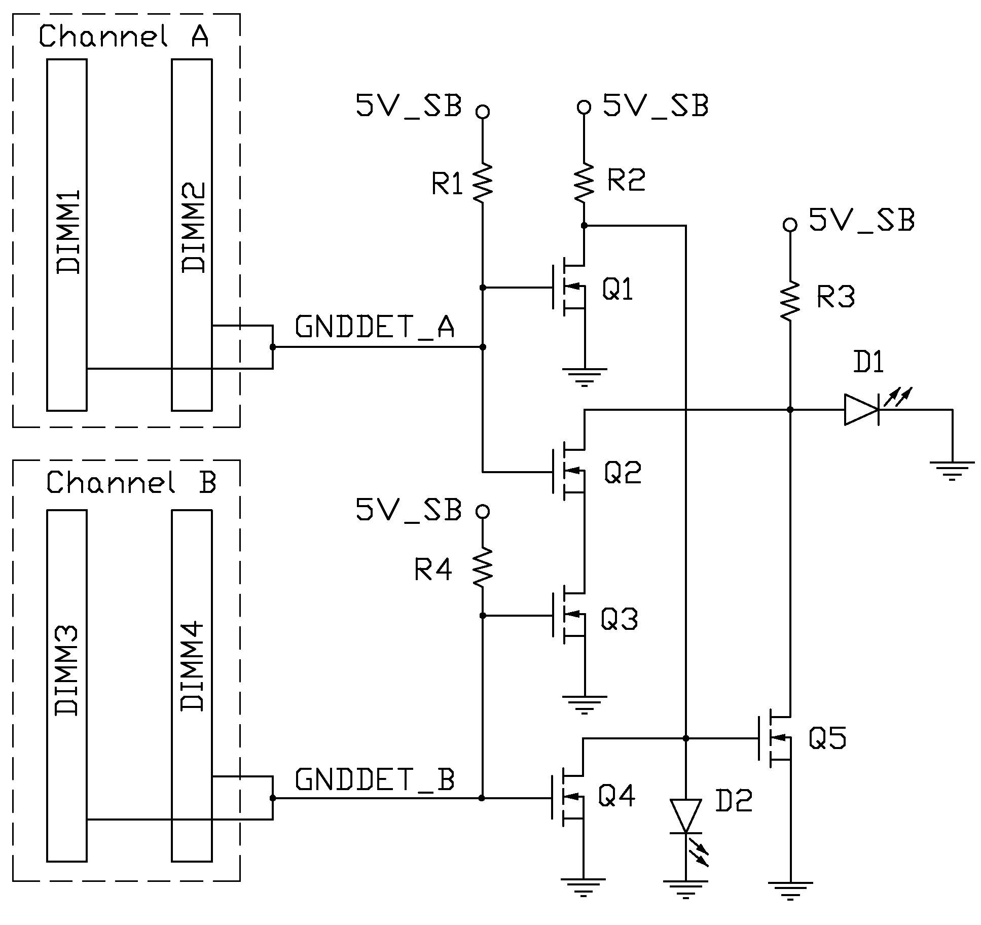
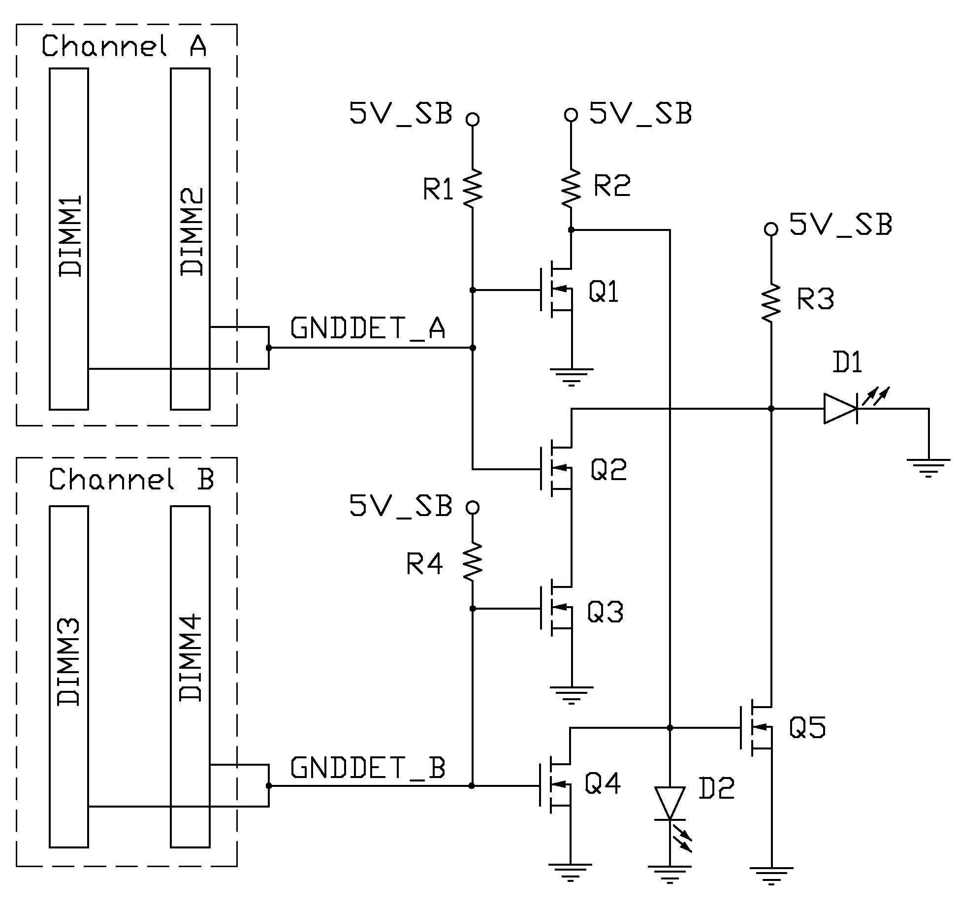
[0008]Referring to the drawing, a memory detecting circuit for a motherboard in accordance with an embodiment of the present invention includes five N type metal oxide semiconductor (NMOS) transistors Q1˜Q5, four resistors R1˜R4, and two light emitting diodes D1 and D2.

[0009]The gate of the NMOS transistor Q1 is arranged to receive a standby power 5V_SB provided by the motherboard via the resistor R1, and also connected to ground lines of two memory sockets DIMM1 and DIMM2 to receive a first memory detecting signal GNDDET_A. The drain of the NMOS transistor Q1 is arranged to receive the standby power 5V_SB via the resistor R2. The source of the NMOS transistor Q1 is grounded. The gates of the NMOS transistors Q1 and Q2 are connected to each other. The drain of the NMOS transistor Q2 is arranged to receive the standby power 5V_SB via the resistor R3, and also connected to the anode of the light emitting diode D1. The source of the NMOS transistor Q2 is connected to the drain of the N...


PUM


Abstract

A memory detecting circuit includes five switch elements and two indication devices. A first switch element is connected to a standby power, and also connected to memory sockets of a first channel to receive a first memory detecting signal. A second switch element is connected to the first switch element and the standby power. A third switch element is connected to the second switch element and the standby power, and also connected to memory sockets of a second channel to receive a second memory detecting signal. A fourth switch element is connected to the third switch element and the standby power. A fifth switch element is connected to the fourth switch element and the standby power. When there are memories installed into the memory sockets of the first channel and the second channel, the second indication device indicates that the memories run in a dual channel mode.

Description

BACKGROUND[0001]1. Field of the Invention[0002]The present invention relates to detecting circuits and, particularly, to a memory detecting circuit for a motherboard.[0003]2. Description of the Related Art[0004]In a computer system, a central processing unit (CPU) reads data faster than a random access memory (RAM) can deliver, and usually the CPU has to wait for the RAM to deliver data. When the RAM is unable to keep up with the CPU, however, a bottleneck occurs, leaving the CPU with nothing to process. Under a single channel mode, any CPU with a bus speed greater than the RAM speed would be susceptible to the bottleneck effect. A dual channel mode is a technique used to alleviate the problem by doubling the amount of the available memory bandwidth. Instead of the single channel mode, a second parallel channel is added in the dual channel mode. With two channels working simultaneously, the bottleneck effect is reduced. Rather than waiting for the memory technology to improve, the d...

Claims


Application Information

Patent Timeline
Patent Type & Authority Patents(United States)
IPC IPC(8): G11C7/00
CPCG11C5/143G11C5/04
Inventor LI, BING-JIANWANG, NINGYOU, YONG-XING
Owner HONG FU JIN PRECISION IND (SHENZHEN) CO LTD
Why Eureka
Try Eureka