Method of monitoring process misalignment to reduce asymmetric device operation and improve the electrical and hot carrier performance of LDMOS transistor arrays

a technology of ldmos transistor array and process misalignment, which is applied in the direction of semiconductor/solid-state device testing/measurement, semiconductor/solid-state device details, instruments, etc., can solve the problems of series on-resistance and substrate current degrade (increase), hot carriers, and a number of device parameters

Active Publication Date: 2010-05-18
NAT SEMICON CORP
View PDF5 Cites 16 Cited by
  • Summary
  • Abstract
  • Description
  • Claims
  • Application Information

AI Technical Summary

Problems solved by technology

Hot carriers, however, degrade a number of device parameters over time.
For example, the series on-resistance and the substrate current degrade (increase) with time as a result of hot carrier damage.
Degradation in the series on-resistance and substrate current leads to increased device series resistance and heat dissipation, eventually leading to device failure.
The n-channel LDMOS (NLDMOS) transistor is particularly prone to early failure due to increased series on-resistance and substrate current resulting from hot carrier damage.
However, process misalignment biases that occur during the manufacturing process can cause n− drain extension region 116 to be shifted either right or left which, in turn, leads to asymmetric device operation.
This asymmetric device operation adversely impacts electrical device parameters, such as breakdown voltage, on-resistance, substrate current and device hot carrier reliability.

Method used


Image

  • Method of monitoring process misalignment to reduce asymmetric device operation and improve the electrical and hot carrier performance of LDMOS transistor arrays
  • Method of monitoring process misalignment to reduce asymmetric device operation and improve the electrical and hot carrier performance of LDMOS transistor arrays
  • Method of monitoring process misalignment to reduce asymmetric device operation and improve the electrical and hot carrier performance of LDMOS transistor arrays

Examples


Embodiment Construction

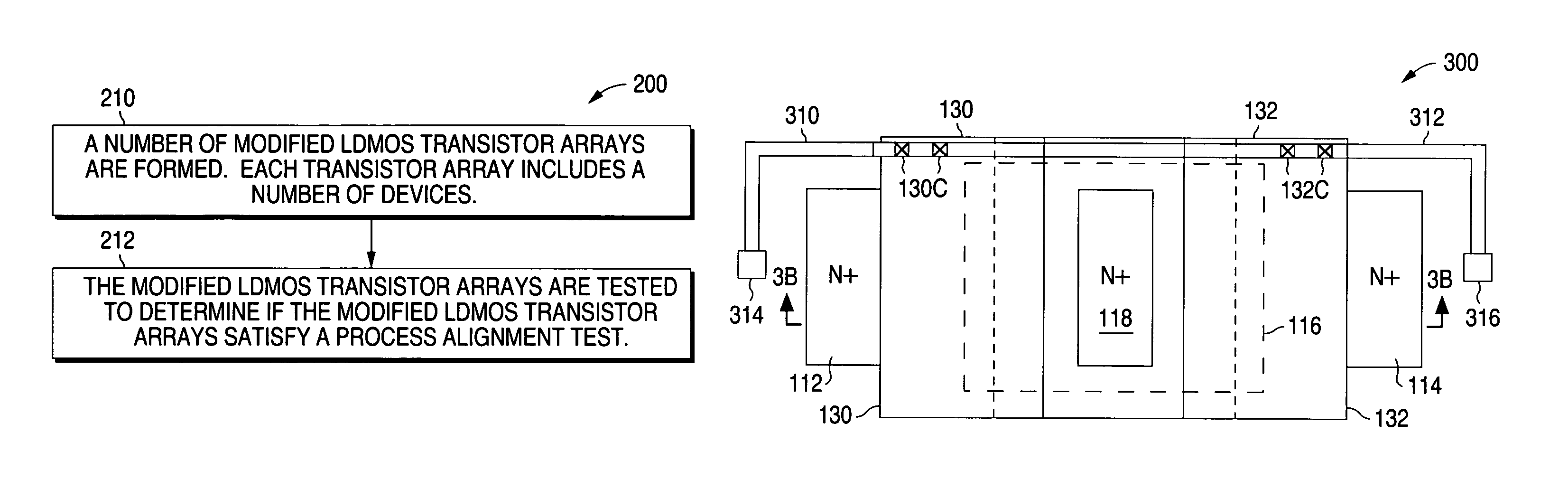
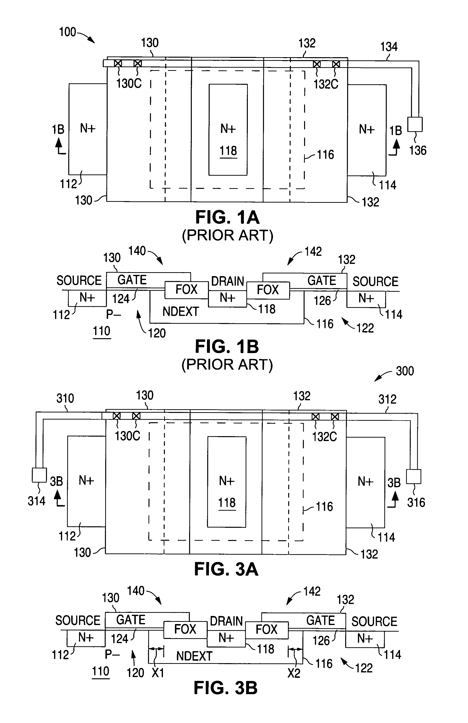
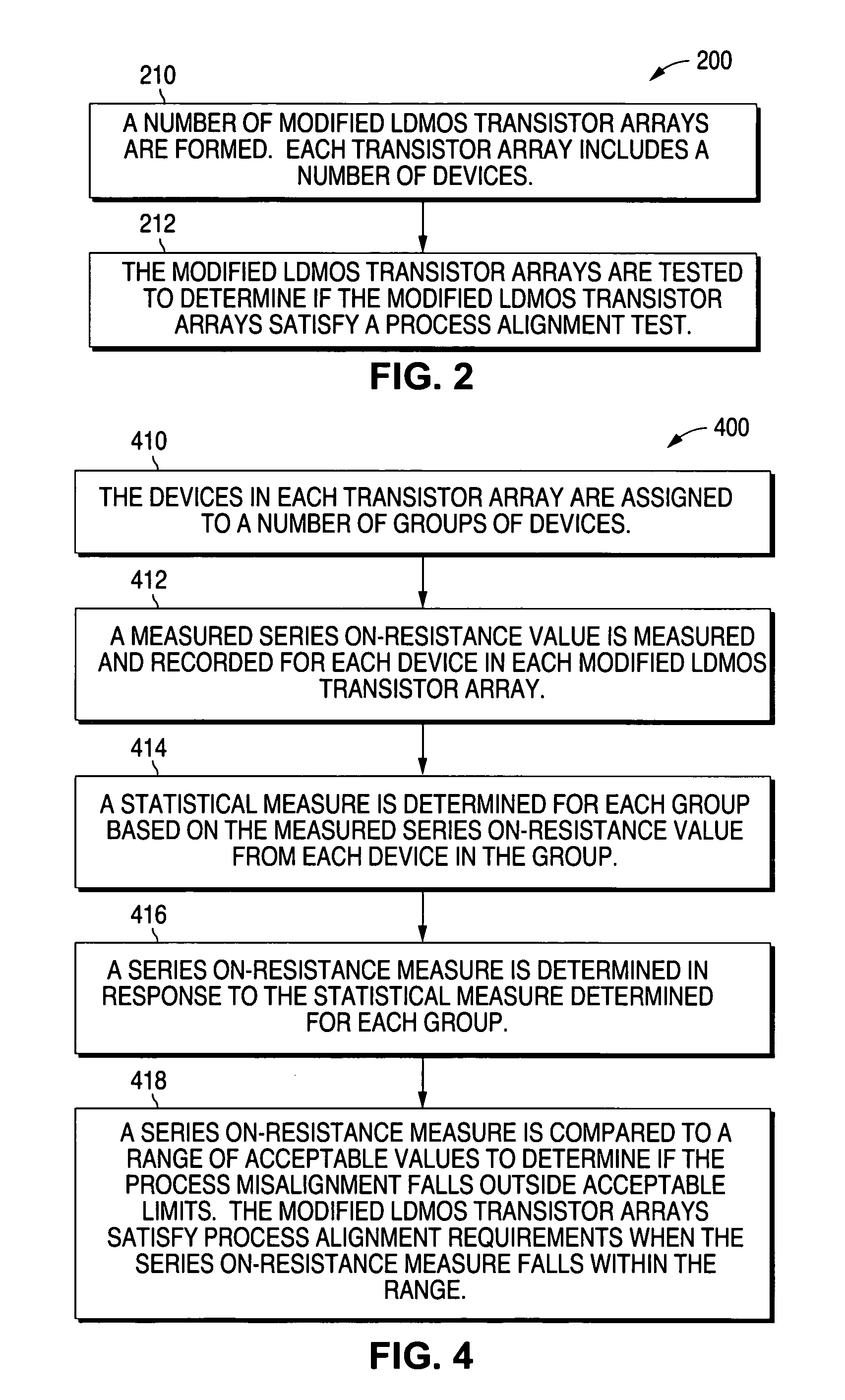
[0027]FIG. 2 shows a flow chart that illustrates an example of a method 200 of testing lateral DMOS (LDMOS) transistor arrays in accordance with the present invention. As described in greater detail below, the present invention measures the substrate currents, series on-resistances, breakdown voltages and hot carrier performance of the devices in a LDMOS transistor array.

[0028]Device misalignment biases result in undesired asymmetric electrical operation and reliability between the devices in the LDMOS array. The present invention measures these asymmetries and utilizes the electrical measurements to quantify and provide information on effective process misalignment so that manufacturing process biases can be minimized to acceptable values. Minimizing these alignment biases improves electrical performance (especially breakdown voltage) and device reliability.

[0029]As shown in FIG. 2, method 200 begins at 210 where a number of modified LDMOS transistor arrays are formed. Each LDMOS t...


PUM


Abstract

A number of modified lateral DMOS (LDMOS) transistor arrays are formed and tested to determine if a measured value, such as a series on-resistance, substrate current, breakdown voltage, and reliability, satisfies process alignment requirements. The modified LDMOS transistor arrays are similar to standard LDMOS transistor arrays such that the results of the modified LDMOS transistor arrays can be used to predict the results of the standard LDMOS transistor arrays.

Description

BACKGROUND OF THE INVENTION[0001]1. Field of the Invention[0002]The present invention relates to LDMOS transistor arrays and, more particularly, to a method of monitoring mask misalignment biases of key LDMOS process steps. By characterizing these offsets, process biases can be eliminated, leading to improved electrical and hot carrier reliability performance of LDMOS arrays.[0003]2. Description of the Related Art[0004]A lateral DMOS (LDMOS) transistor array is a well known semiconductor structure that is commonly used in high power applications. FIGS. 1A-1B show views that illustrate a prior-art, dual-device LDMOS transistor array 100. FIG. 1A shows a plan view, while FIG. 1B shows a cross-sectional view taken along lines 1B-1B of FIG. 1A.[0005]As shown in FIGS. 1A and 1B, array 100 includes a p− semiconductor material 110, such as an epitaxial layer or a substrate, and spaced-apart first and second n+ source strips 112 and 114 that are formed in material 110. Further, array 100 in...

Claims


Application Information

Patent Timeline
Patent Type & Authority Patents(United States)
IPC IPC(8): G01R31/26G06F17/18G06F17/50
CPCH01L22/34H01L29/7835
Inventor BRISBIN, DOUGLASCHAPARALA, PRASAD
Owner NAT SEMICON CORP
Why Eureka
Try Eureka