Pulsed-plasma system with pulsed sample bias for etching semiconductor substrates

a plasma etching and sample bias technology, applied in the direction of electrical discharge tubes, decorative arts, electrical equipment, etc., can solve the problems of plasma etching with respect, equipment and processes used to fabricate ics scale without problems, and limitations of plasma etching process have revealed themselves

Active Publication Date: 2010-05-18
APPLIED MATERIALS INC
View PDF21 Cites 89 Cited by
  • Summary
  • Abstract
  • Description
  • Claims
  • Application Information

AI Technical Summary

Benefits of technology

[0005]In order to pattern semiconductor stacks into meaningful structures, a lithography / etch process is typically employed. State-of-the-art etch processes include etching a semiconductor stack with a system comprising an ionized gas, i.e. a plasma. Plasma etch processing may be particularly useful for etching multiple adjacent structures with fine features. However, as demands on feature size and spacing become more stringent, limitations of the plasma etch process have revealed themselves.

Problems solved by technology

However, it is seldom the case that the equipment and processes used to fabricate ICs scale without issue.
However, as demands on feature size and spacing become more stringent, limitations of the plasma etch process have revealed themselves.
One potential limitation of plasma etching may be with respect to the fabrication of an IC with variable spacing between various semiconductor structures within a single sample.
In some cases, this over-etch may have a detrimental impact on the resultant semiconductor structures.

Method used


Image

  • Pulsed-plasma system with pulsed sample bias for etching semiconductor substrates
  • Pulsed-plasma system with pulsed sample bias for etching semiconductor substrates
  • Pulsed-plasma system with pulsed sample bias for etching semiconductor substrates

Examples


Embodiment Construction

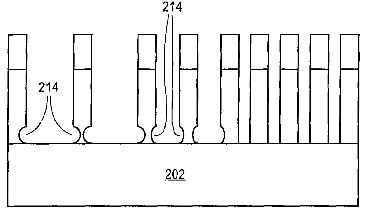
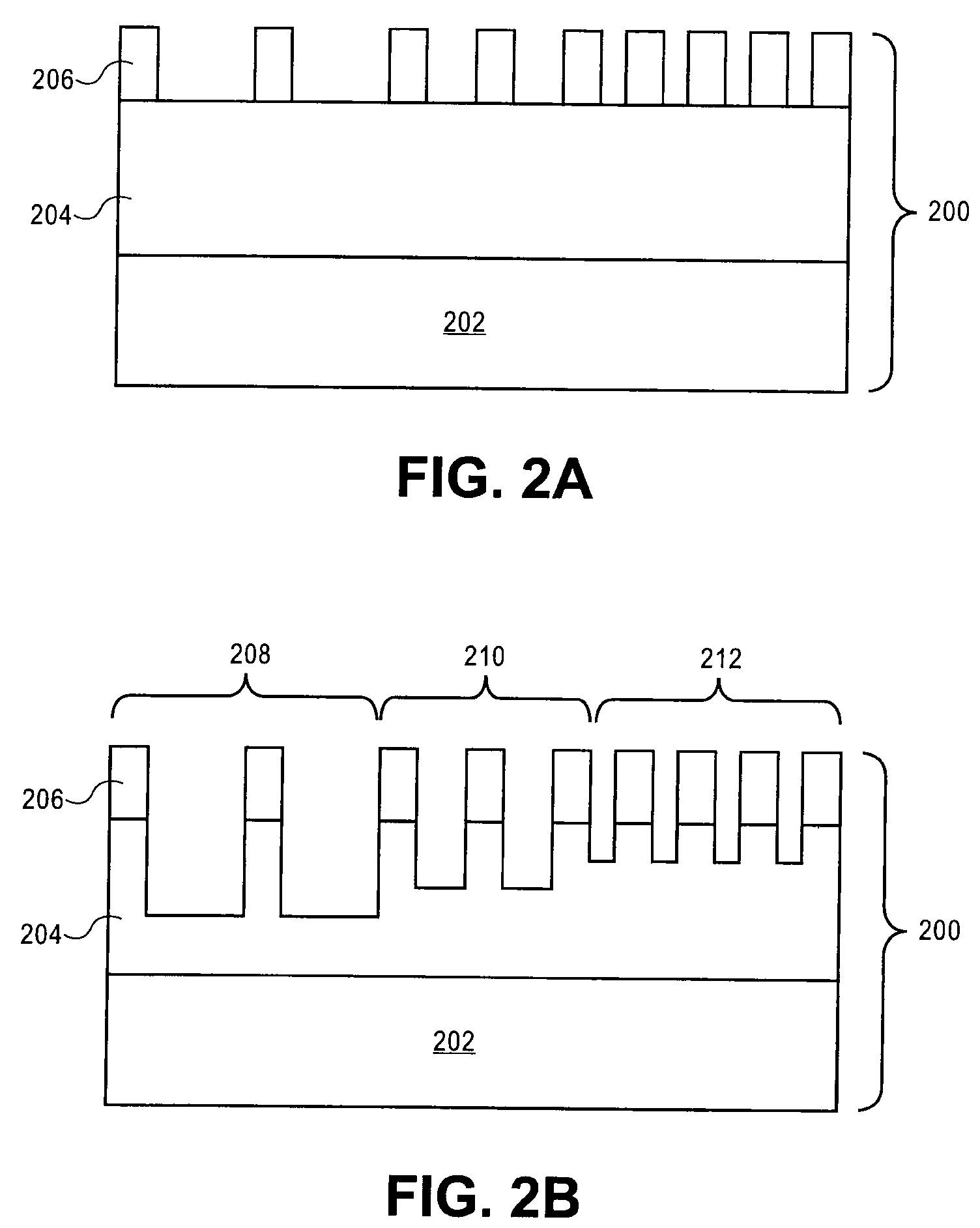
[0021]A method and a system for etching semiconductor structures are described. In the following description, numerous specific details are set forth, such as specific dimensions and chemical regimes, in order to provide a thorough understanding of the present invention. It will be apparent to one skilled in the art that the present invention may be practiced without these specific details. In other instances, well-known processing steps, such as patterning steps or wet chemical cleans, are not described in detail in order to not unnecessarily obscure the present invention. Furthermore, it is understood that the various embodiments shown in the figures are illustrative representations and are not necessarily drawn to scale.

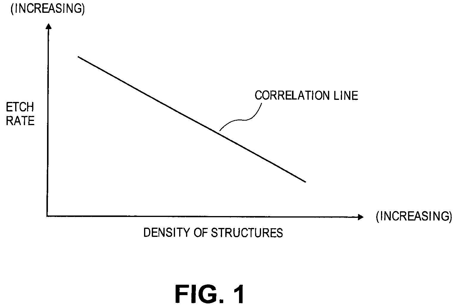
[0022]Disclosed herein are a pulsed plasma method and a corresponding system for etching semiconductor structures. A portion of a sample may be removed by applying a pulsed plasma process, wherein the pulsed plasma process comprises a plurality of duty cycles. In ...


PUM

PropertyMeasurementUnit
poweraaaaaaaaaa
frequencyaaaaaaaaaa
pressureaaaaaaaaaa

Abstract

A pulsed plasma system with pulsed sample bias for etching semiconductor structures is described. In one embodiment, a portion of a sample is removed by applying a pulsed plasma process, wherein the pulsed plasma process comprises a plurality of duty cycles. A negative bias is applied to the sample during the ON state of each duty cycle, while a zero bias is applied to the sample during the OFF state of each duty cycle. In another embodiment, a first portion of a sample is removed by applying a continuous plasma process. The continuous plasma process is then terminated and a second portion of the sample is removed by applying a pulsed plasma process.

Description

BACKGROUND OF THE INVENTION[0001]1) Field of the Invention[0002]The invention is in the fields of Semiconductor Structures and Semiconductor Equipment.[0003]2) Description of Related Art[0004]For the past several years, the performance and capabilities of integrated circuits (ICs), e.g. logic circuits for computation and memory circuits for information storage, have been greatly enhanced by scaling the features of semiconductor structures to ever smaller dimensions. However, it is seldom the case that the equipment and processes used to fabricate ICs scale without issue. Continued advances in both semiconductor process technologies as well as in the equipment used to carry out such processes has ensured survival of the relentless pursuit of scaling by the Semiconductor Industry.[0005]In order to pattern semiconductor stacks into meaningful structures, a lithography / etch process is typically employed. State-of-the-art etch processes include etching a semiconductor stack with a system...

Claims


Application Information

Patent Timeline
Patent Type & Authority Patents(United States)
IPC IPC(8): H01L21/302
CPCH01L21/3065H01L21/31116C23F4/00H01J37/32009H01L21/32137
Inventor KIM, TAE WONLEE, KYEONG-TAEPATERSON, ALEXANDERTODOROV, VALENTIN N.DESHMUKH, SHASHANK C.
Owner APPLIED MATERIALS INC
Why Eureka
Try Eureka