Flat panel display and driving method using the same

a technology of organic light and display, applied in the direction of discharge tube luminescnet screen, organic semiconductor device, instruments, etc., can solve the problems of power consumption increase, limit on increasing the width of the channel of tft, and the light emitting device of the transparent organic light emitting display deteriorates

Active Publication Date: 2010-05-18
SAMSUNG DISPLAY CO LTD
View PDF19 Cites 153 Cited by
  • Summary
  • Abstract
  • Description
  • Claims
  • Application Information

AI Technical Summary

Problems solved by technology

Because these materials are not transparent, there is limitation on increasing a width of a channel of the TFT when these opaque materials are used to manufacture a TFT that is used as a switching device of a transparent organic light emitting display.
Therefore, there has problems that the light emitting device of the transparent organic light emitting display deteriorates and power consumption increases.
Also, it is not possible to display an image on both surfaces of the organic light emitting display, because an amount of light passing through the opaque TFT is blocked by the TFT.

Method used


Image

  • Flat panel display and driving method using the same
  • Flat panel display and driving method using the same
  • Flat panel display and driving method using the same

Examples


first embodiment

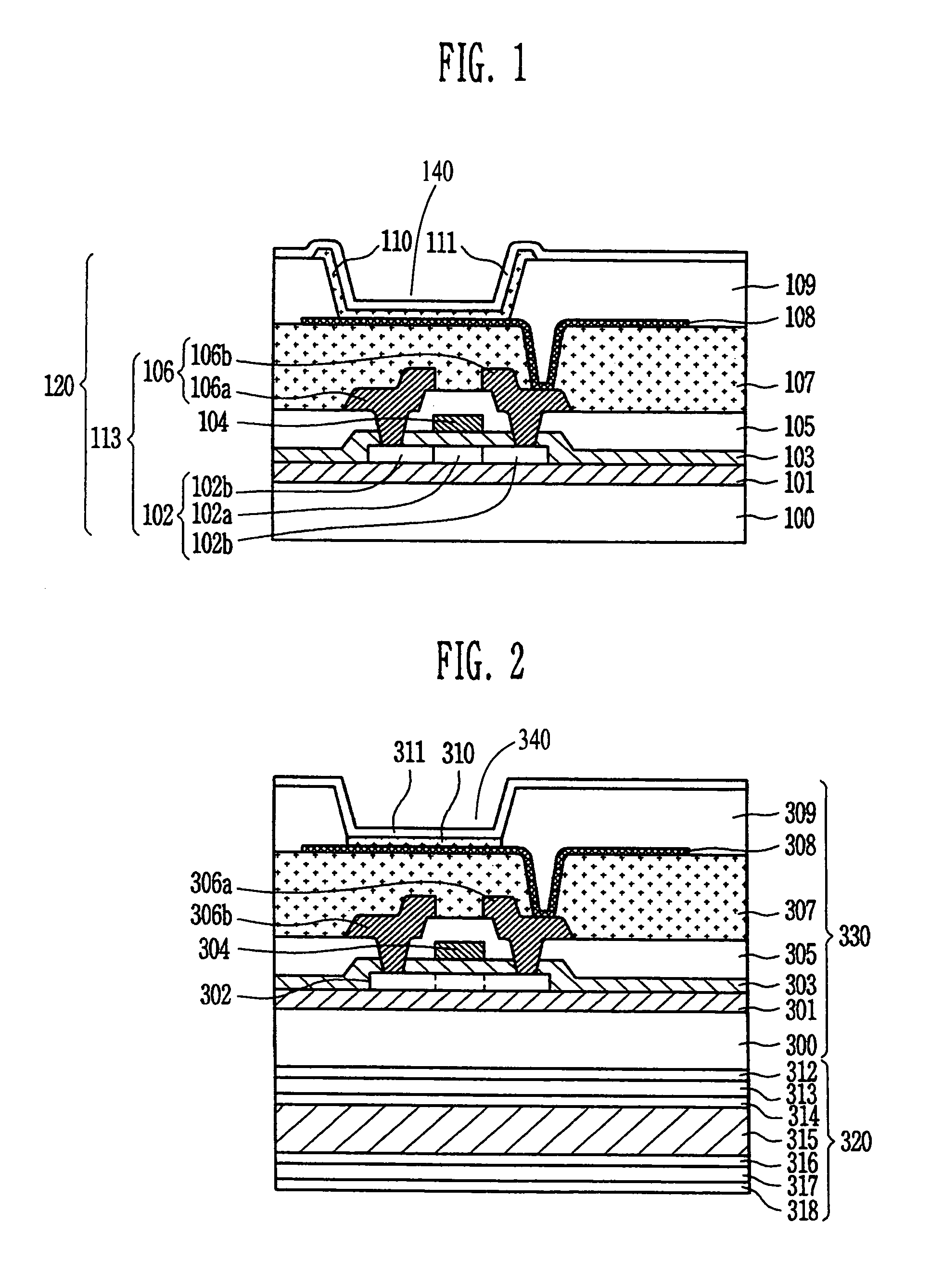
[0026]FIG. 2 is a schematic sectional view illustrating an organic light emitting display constructed as the present invention. Referring to FIG. 2, the organic light emitting display includes display unit 330 that includes at least one organic light emitting diode and a thin film transistor formed on first transparent substrate 300, and controlling unit 320 formed on the lower portion of display unit 330 to control transmission of light emitted from display unit 330.

[0027]Hereinafter, controlling unit 320 will be described in detail. First substrate 313 and second substrate 317 of controlling unit 320 are arranged in a manner that an inner surface of first substrate 313 and an inner surface of second substrate 317 face each other. First transparent electrode 314 and second transparent electrode 316 are formed in the inner surfaces of first substrate 313 and second substrate 317, respectively. Liquid crystal layer 315, which is a light shielding layer, is interposed between first tr...

second embodiment

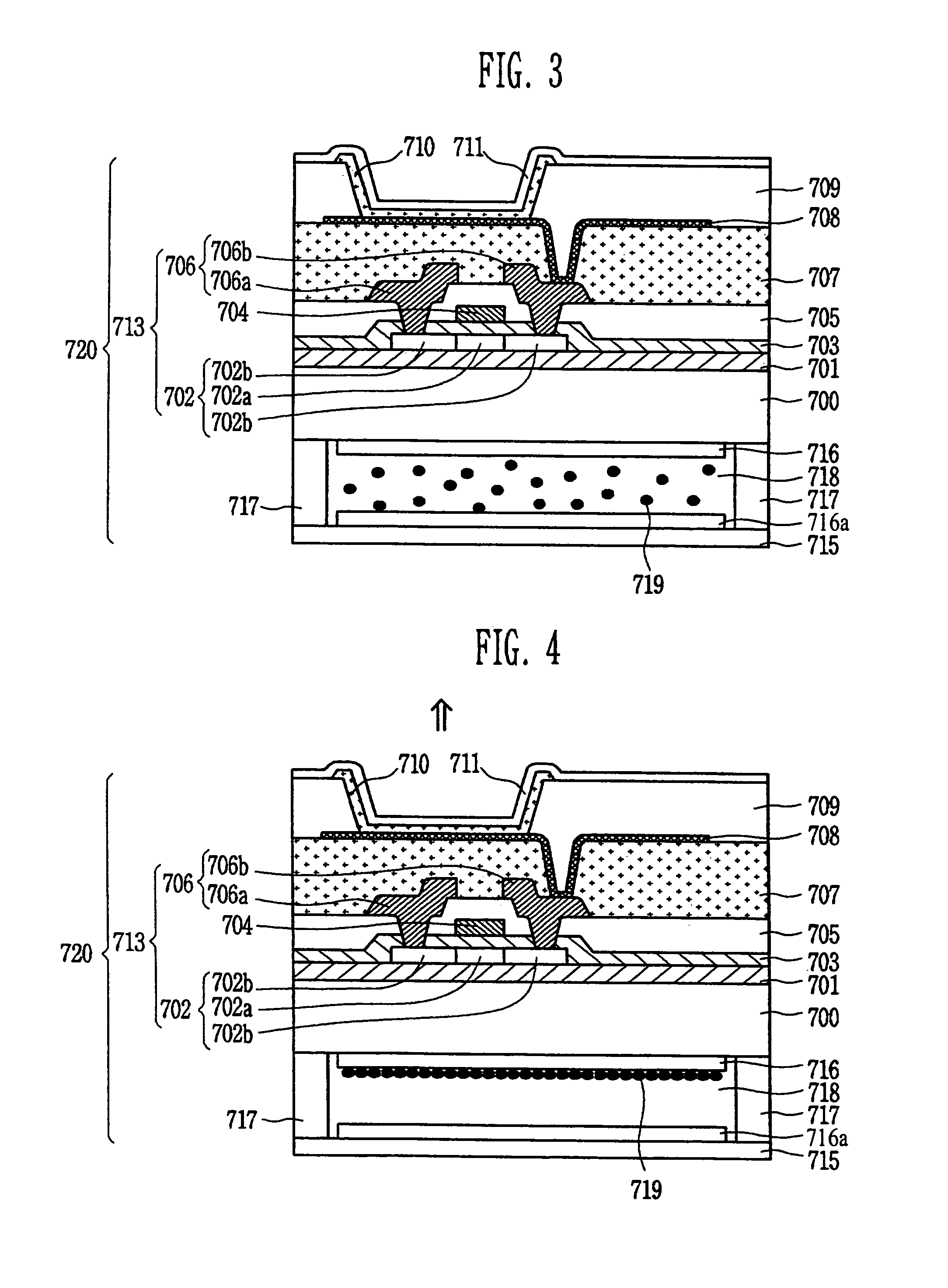
[0046]FIG. 3 is a schematic sectional view illustrating an organic light emitting display constructed as the present invention. As shown in FIG. 3, at least one transparent thin film transistor 713 and a structure including emission layer 710 are formed on the upper surface of first transparent substrate 700 of organic light emitting display 720. An electrophoretic device, which is a controlling unit, is formed at the lower surface of first transparent substrate 700.

[0047]Transparent thin film transistor 713 includes semiconductor layer 702, gate electrode 704, and electrode 706. Semiconductor layer 702 includes active layer 702a and ohmic contact layers 702b, and electrode 706 includes source electrode 706a and drain electrode 706b. The structure of transparent thin film transistor 713 is the same as described referring to FIG. 2, and detailed description of transparent thin film transistor 713 will be omitted.

[0048]The electrophoretic device is a non-emission type display device, ...

third embodiment

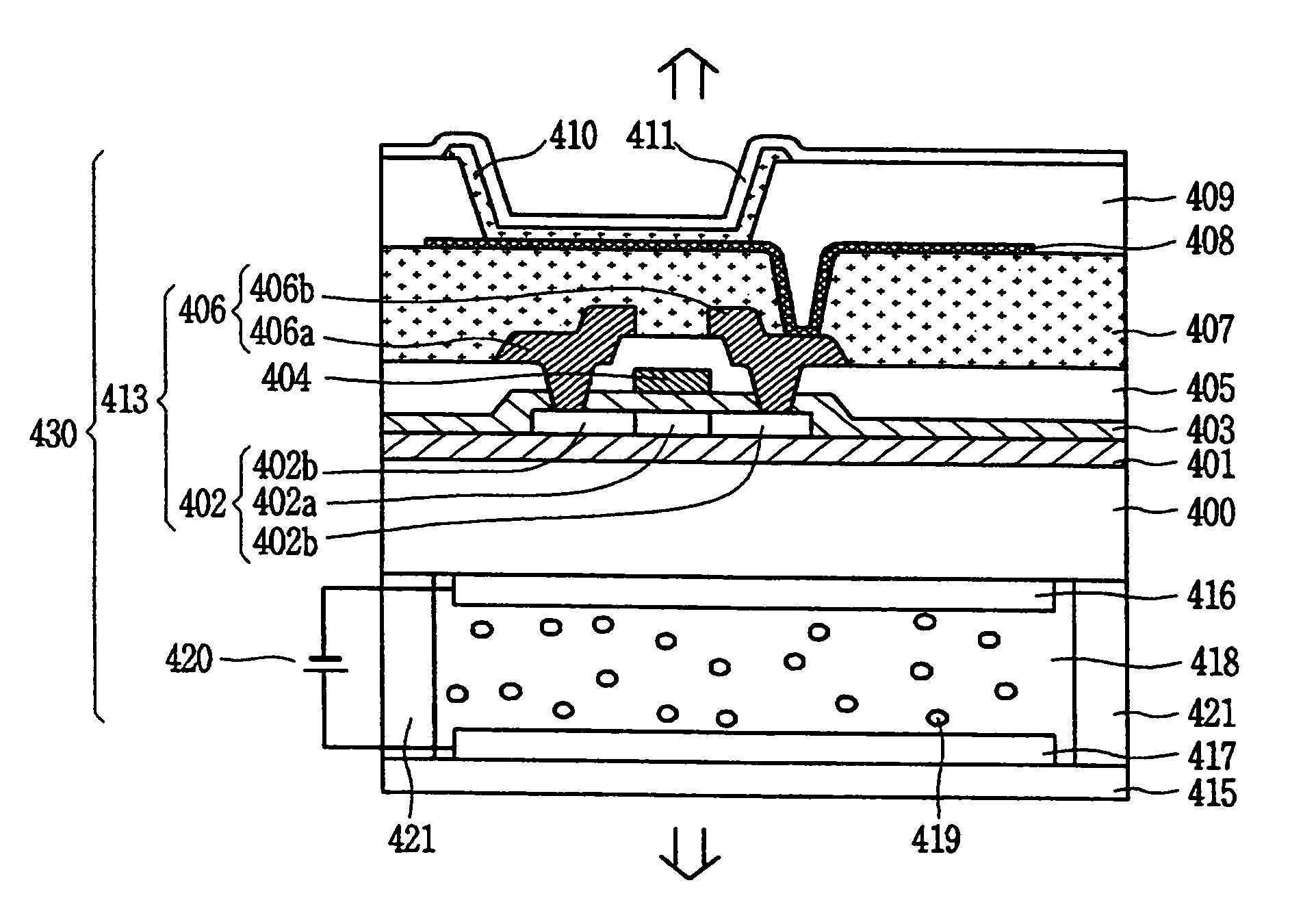
[0065]FIG. 6 is a schematic sectional view illustrating an organic light emitting display (OLED) constructed as the present invention. As shown in FIG. 6, at least one transparent TFT 413 and a structure including emission layer 410 are constructed on the upper surface of first transparent substrate 400 of OLED 430 of the present invention. Instead of the electrophoretic device as shown in FIGS. 3-5, an electrochromic device, which is a controlling unit, is formed on the lower surface of substrate 400.

[0066]Transparent thin film transistor 413 includes semiconductor layer 402, gate electrode 404, and electrode 406. Semiconductor layer 402 includes active layer 402a and ohmic contact layers 402b, and electrode 406 includes source electrode 406a and drain electrode 406b. The structure of transparent thin film transistor 413 is the same as described referring to FIG. 2, and detailed description of transparent thin film transistor 413 will be omitted.

[0067]In general, electrochromism is...


PUM


Abstract

An organic light emitting display (OLED), which includes a display unit and a controlling unit, is provided. The display unit includes an organic light emission layer and a transparent thin film transistor (TFT) to drive the organic light emission layer, and the display unit emits light into two opposite surfaces (upper and lower surfaces). The controlling unit includes an electro-optical layer that is capable of being switched from one state to another state by applying voltage to the layer. The controlling unit controls transmission of light emitted from the display unit. Therefore the flat panel display of the present invention is capable of displaying an image in one surface or in two surfaces. The selection of surface of image display can be manually or automatically controlled by a user. The controlling unit can includes a liquid crystal device, an electrophoretic device, or an electrochromic device.

Description

CLAIM OF PRIORITY[0001]This application makes reference to, incorporates the same herein, and claims all benefits accruing under 35 U.S.C. §119 from an application for FLAT PANEL DISPLAY AND DRIVING METHOD USING THE SAME earlier filed in the Korean Intellectual Property Office on 21 Dec. 2005 and there duly assigned Serial No. 2005-127223.BACKGROUND OF THE INVENTION[0002]1. Field of the Invention[0003]The present invention relates to an organic light emitting display, and more particularly, to an organic light emitting display that is capable of displaying an image in one surface (an upper surface) or in two surfaces (an upper and a lower surfaces). The surface of image display can be selected by a user, and can be selected for a time period set by a user. The organic light emitting display of the present invention has a controlling unit that changes between an opaque state and a transparent state, and the controlling unit controls transmission of light to display an image on one su...

Claims


Application Information

Patent Timeline
Patent Type & Authority Patents(United States)
IPC IPC(8): H01J63/04
CPCH01L27/3244H01L27/3232G02F2201/44H01L2251/5323H10K59/50H10K2102/3031H10K59/128H10K59/126H05B33/22H10K59/12
Inventor JIN, DONG-UNJEONG, JAE-KYEONGSHIN, HYUN-SOOMO, YEON-GON
Owner SAMSUNG DISPLAY CO LTD
Why Eureka
Try Eureka