Graded junction silicon nanocrystal embedded silicon oxide electroluminescence device

a silicon oxide and nanocrystal technology, applied in the field of integrated circuit (ic) fabrication, can solve the problems of difficult balancing all of these interactions within a single homogeneous film, the material that is efficient in transporting charge carriers is not necessarily efficient in allowing excitons to decay into light emission, and the material cannot support the radiative decay of excitons with the same efficiency. , to achieve the effect of enhancing chemical vapor deposition and enhancing optical emission

Inactive Publication Date: 2010-05-25
SHARP KK
View PDF6 Cites 3 Cited by
  • Summary
  • Abstract
  • Description
  • Claims
  • Application Information

AI Technical Summary

Problems solved by technology

Based on empirical data, it has been determined that the balancing all of these interactions is difficult within a single homogeneous film.
A nc-Si in-oxide material that is efficient in transporting charge carriers is not necessarily efficient in allowing excitons to decay into light emission.
Generating sufficient current to form excitons on nc-Si particles is facilitated using a high nc-Si in-oxide concentration material, but this same material will not support the radiative decay of excitons with the same efficiency as a lower concentration nc-Si Si oxide material.

Method used


Image

  • Graded junction silicon nanocrystal embedded silicon oxide electroluminescence device
  • Graded junction silicon nanocrystal embedded silicon oxide electroluminescence device
  • Graded junction silicon nanocrystal embedded silicon oxide electroluminescence device

Examples


Embodiment Construction

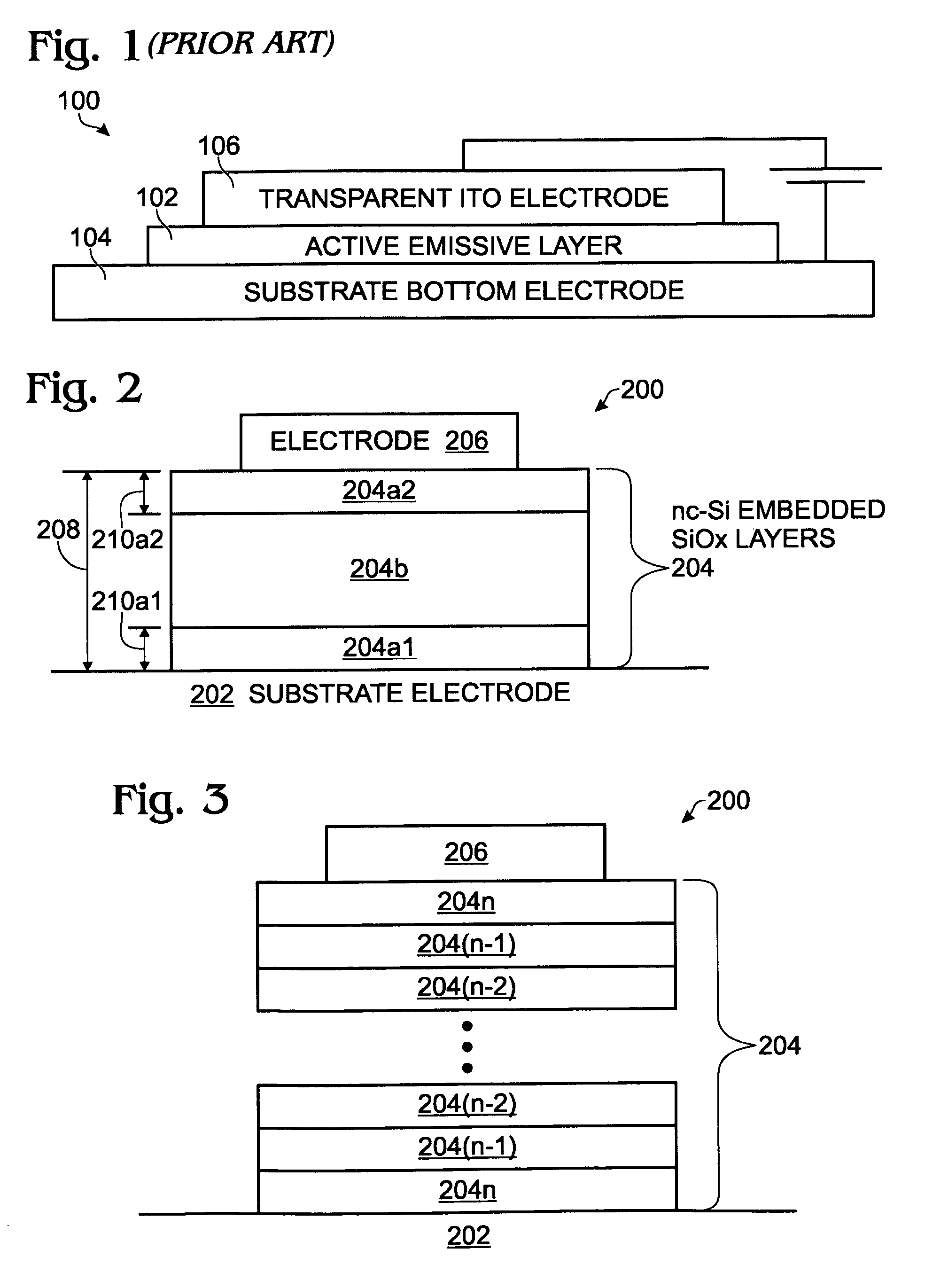
[0029]FIG. 2 is a partial cross-sectional view of a Si nanocrystal embedded Si oxide electroluminescence (EL) device. The EL device 200 comprises a substrate bottom electrode 202. A plurality of Si nanocrystal embedded SiOx film layers 204 overlie the bottom electrode 202, where X is less than 2, and where outside film layers 204a1 and 204a2 sandwich an inner film layer 204b having a lower concentration of Si nanocrystals. The Si nanocrystal embedded SiOx film layers are also referred to herein as nc-Si SiOX film layers, or nc-Si embedded SiOX film layers. A transparent top electrode 206 overlies the plurality of Si nanocrystal embedded SiOx film layers. ITO is an example of a transparent electrode. Other examples include thin metal layers.

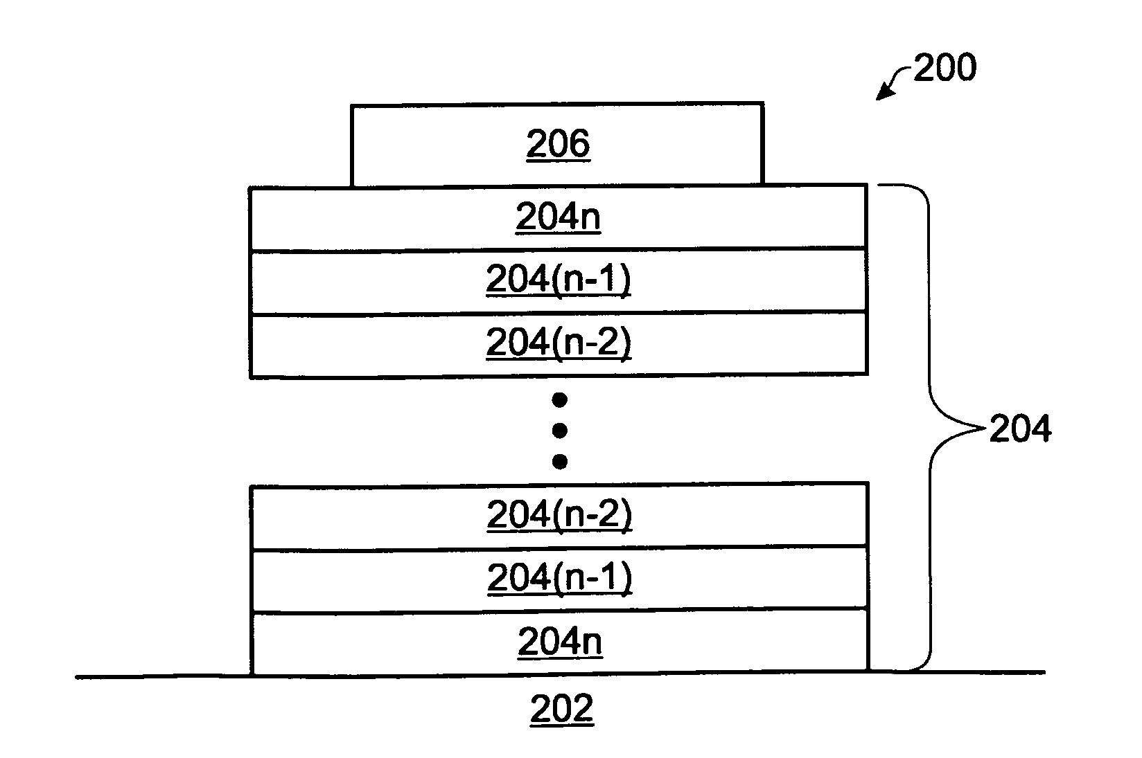
[0030]FIG. 3 is a partial cross-sectional view of a first variation of the Si nanocrystal embedded Si oxide EL device of FIG. 2. More generally, the EL device 200 is not limited to just three Si nanocrystal embedded Si oxide layers. In this aspect...


PUM

PropertyMeasurementUnit
frequencyaaaaaaaaaa
pressureaaaaaaaaaa
thicknessaaaaaaaaaa

Abstract

A silicon (Si) nanocrystal embedded Si oxide electroluminescence (EL) device and associated fabrication process are presented. The method provides a substrate bottom electrode, and forms a plurality of Si nanocrystal embedded SiOx film layers overlying the bottom electrode, where X is less than 2. Each SiOx film layer has a Si excess concentration in a range of about 5 to 30%. The outside film layers sandwich an inner film layer having a lower concentration of Si nanocrystals. Alternately stated, the outside Si nanocrystal embedded SiOx film layers have a higher electrical conductivity than a sandwiched inner film layer. A transparent top electrode is formed over the plurality of Si nanocrystal embedded SiOx film layers. The plurality of Si nanocrystal embedded SiOx film layers are deposited using a high density plasma-enhanced chemical vapor deposition (HD PECVD) process. The HD PECVD process initially deposits SiOx film layers, which are subsequently annealed.

Description

RELATED APPLICATIONS[0001]This application is a continuation-in-part of a pending patent application entitled, LIGHT EMITTING DEVICE WITH A NANOCRYSTALLINE SILICON EMBEDDED INSULATOR FILM, invented by Huang et al., Ser. No. 12 / 126,430, filed May 23, 2008, which is a Continuation-in-Part of:[0002]a pending patent application entitled, SILICON OXIDE THIN-FILMS WITH EMBEDDED NANOCRYSTALLINE SILICON, invented by Pooran Joshi et al., Ser. No. 11 / 418,273, filed May 4, 2006 now U.S. Pat. No. 7,544,625, which is a Continuation-in-Part of the following applications:[0003]ENHANCED THIN-FILM OXIDATION PROCESS, invented by Pooran Joshi et al., Ser. No. 11 / 327,612, filed Jan. 6, 2006;[0004]HIGH-DENSITY PLASMA HYDROGENATION, invented by Pooran Joshi et al., Ser. No. 11 / 013,605, filed Dec. 15, 2004 now U.S. Pat. No. 7,446,023;[0005]DEPOSITION OXIDE WITH IMPROVED OXYGEN BONDING, invented by Pooran Joshi, Ser. No. 10 / 801,377, filed Mar. 15, 2004 now U.S. Pat. No. 7,122,487;[0006]HIGH-DENSITY PLASMA ...

Claims


Application Information

Patent Timeline
Patent Type & Authority Patents(United States)
IPC IPC(8): H01L21/00H01J1/62H01L21/20H01J9/24
CPCC23C16/24C23C16/30C23C16/401C23C16/56C23C16/505H01L21/02595H01L21/02532
Inventor CASASANTA, VINCENZOVOUTSAS, APOSTOLOS T.JOSHI, POORAN CHANDRA
Owner SHARP KK
Why Eureka
Try Eureka