Plasma display panel

a technology of display panel and plasma, which is applied in the direction of gas discharge vessel/container, address electrode, gas-filled discharge tube, etc., can solve the problems of address discharge and achieve the effects of reducing power consumption, improving luminous efficiency, and low voltage driving

Inactive Publication Date: 2010-06-01
SAMSUNG SDI CO LTD
View PDF21 Cites 2 Cited by
  • Summary
  • Abstract
  • Description
  • Claims
  • Application Information

AI Technical Summary

Benefits of technology

[0015]The present invention provides a plasma display PDP which can realize low voltage driving, to thus reduce power consumption, and which can improve luminous efficiency through a long gap.

Problems solved by technology

The net potential between the Y electrode and the address electrode is smaller than the originally applied address voltage Va, so that the discharge becomes weak, resulting in dissipation of address discharge.

Method used


Image

  • Plasma display panel
  • Plasma display panel
  • Plasma display panel

Examples


first embodiment

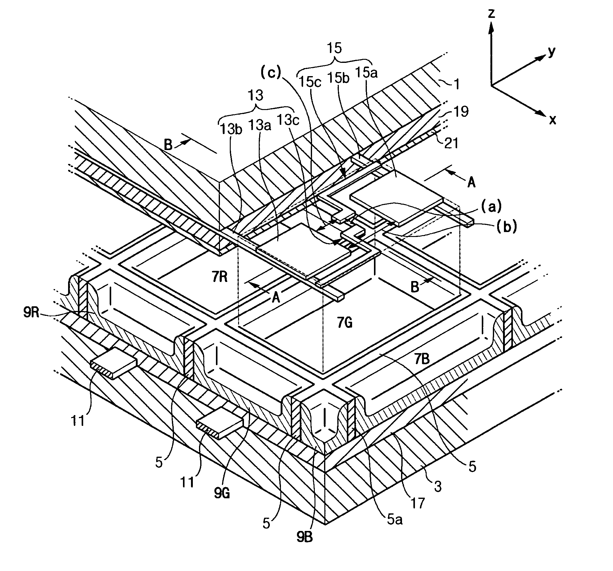
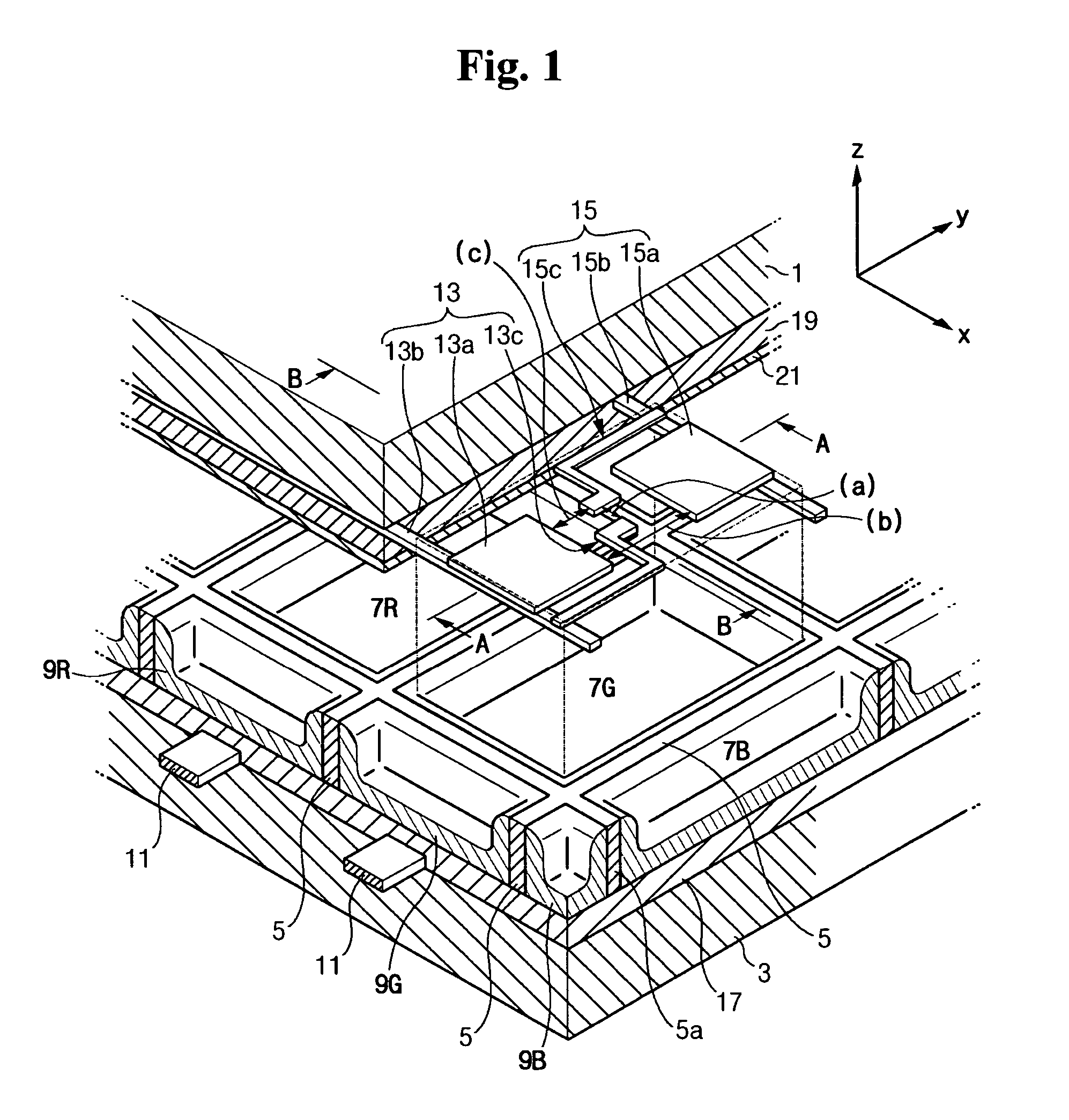
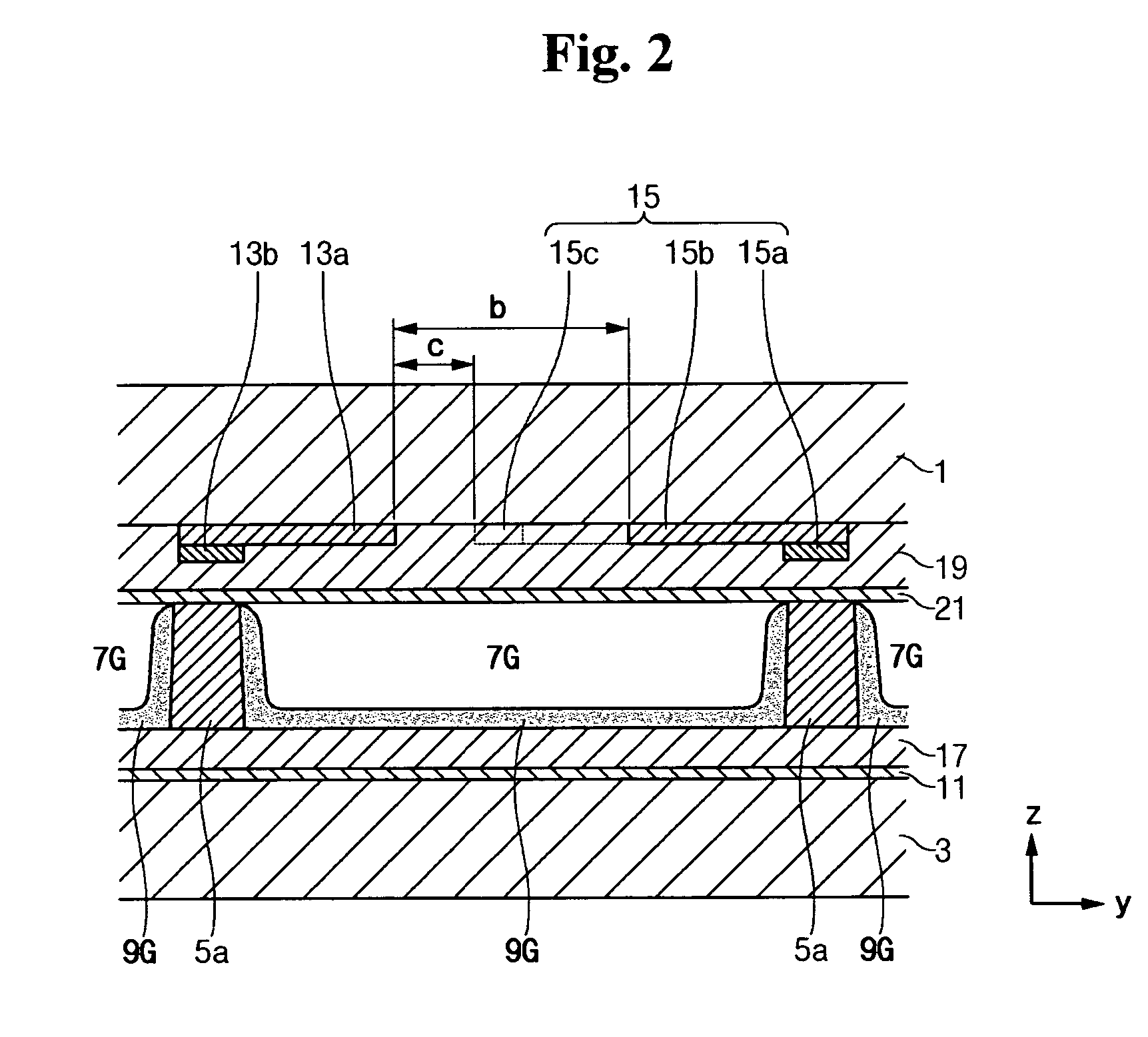
[0034]Turning now to the drawings, referring to FIG. 1, a PDP according to the present invention has a first substrate 1 and a second substrate 3 which are spaced apart at a predetermined distance while facing each other. In the space between both of the substrates 1 and 3, a plurality of discharge cells 7R, 7G, 7B in which plasma discharge takes place are defined by a plurality of barrier ribs 5. Red (R), green (G) and blue (B) phosphors are printed to form phosphor layers 9R, 9G, 9B in the discharge cells 7R, 7G, 7B.

[0035]A plurality of the address electrodes 11 are formed along the y-axis direction of the drawing of the second substrate 3 on a surface of the second substrate 3. A plurality of display electrodes 13 and 15 are formed along the direction intersecting the plurality of address electrodes 11, that is, along the x-axis direction of the drawing, on the second substrate 3.

[0036]Barrier ribs 5 provided in the space between the first substrate 1 and the second substrate 3 a...

second embodiment

[0051]FIG. 5 is a partial plan view of a PDP according to the present invention. The opposing portions 133c′ and 153c′ may be substantially perpendicular to the length direction of the address electrodes 11 (the y-axis direction of the drawing) and may have opposite sides of different lengths. In this case, the pair of opposing portions 133c′ and 153c′ have ends whose facing directions indicated by an arrow “d” cross the length direction of the address electrodes 11 (the y-axis direction) in a slanted manner.

[0052]As described above, the igniter electrodes 13c and 15c, which consist of the expanded portions 131c and 151c, the protruding portions 132c and 152c and the opposing portions 133c and 153c (and 133c′ and 153c′ for the second embodiment), are formed to correspond to the discharge cells 7R, 7G, 7B in the respective barrier ribs 5 adjacent in the direction of the length direction of the bus electrodes 13b and 15b (in the x-axis direction), the igniter electrodes 13c and 15c es...


PUM


Abstract

A plasma display panel (PDP) which can realize low voltage driving, to thus reduce power consumption, and which can improve luminous efficiency through a long gap. The PDP includes a first substrate and a second substrate opposing each other, barrier ribs arranged in a space between the first substrate and the second substrate to define a plurality of discharge cells, phosphor layers formed in each of the plurality of discharge cells, address electrodes formed on the second substrate, and display electrodes provided on the first substrate. The display electrodes include igniter electrodes having ends protruding towards insides of the discharge cells, the igniter electrodes opposing the address electrodes within the discharge cells.

Description

CROSS-REFERENCE TO RELATED APPLICATION[0001]This application claims priority to and the benefit of Korean Patent Application No. 10-2004-0035468 filed in the Korean Intellectual Property Office on May 19, 2004, the entire content of which is incorporated herein by reference.BACKGROUND OF THE INVENTION[0002]1. Field of the Invention[0003]The present invention relates to a plasma display panel (PDP) for display an image.[0004]2. Description of the Related Art[0005]Generally, a PDP is a display device in which vacuum ultraviolet (VUV) rays emitted from the plasma generated by gas discharge excite phosphors to emit red, green, and blue visible light and thereby realize predetermined images. The PDP can provide a large-scale screen of more than 60 inches with a thickness of less than 10 centimeters. Since the PDP is a self emission display device, it typically has no distortion due to view angle and has outstanding color reproduction. Moreover, its manufacturing process is simpler than t...

Claims


Application Information

Patent Timeline
Patent Type & Authority Patents(United States)
IPC IPC(8): H01J17/49H01J11/12H01J11/22H01J11/24H01J11/26H01J11/28H01J11/34H01J11/36H01J17/30
CPCH01J11/12H01J11/24H01J2211/323H01J2211/28H01J2211/245H01J11/28
Inventor KANG, KYOUNG-DOO
Owner SAMSUNG SDI CO LTD
Why Eureka
Try Eureka