Organic electroluminescent device

a technology of electroluminescent devices and organic materials, applied in organic chemistry, organic semiconductor devices, luminescent compositions, etc., can solve the problem of not achieving high-efficiency light emission, and achieve the effect of long life and high efficiency

Active Publication Date: 2015-11-12
PIONEER CORP +2
View PDF4 Cites 10 Cited by
  • Summary
  • Abstract
  • Description
  • Claims
  • Application Information

AI Technical Summary

Benefits of technology

[0020]In order to apply an organic EL element to a display element in a flat panel display or the like, or to a light source, it is necessary to improve the luminous efficiency of the element and also to ensure sufficiently the stability in driving the element. The present invention has an object to provide, in view of the above-mentioned circumstances, a practically useful organic EL element that has high efficiency and high driving stability while being capable of being driven at a low voltage.
[0041]The organic EL element of the present invention uses specific compounds as a mixed host, and hence has lowest excited triplet energy high enough to confine the lowest excited triplet energy of a phosphorescent light-emitting molecule while being capable of being driven at a low voltage. Accordingly, the outflow of energy from the inside of its light-emitting layer does not occur, and the element can achieve high efficiency and a long lifetime.

Problems solved by technology

After that, investigations have been made on using a europium complex as an attempt to use a triplet excited state, but highly efficient light emission has not been accomplished.

Method used


Image

  • Organic electroluminescent device
  • Organic electroluminescent device
  • Organic electroluminescent device

Examples


example 1

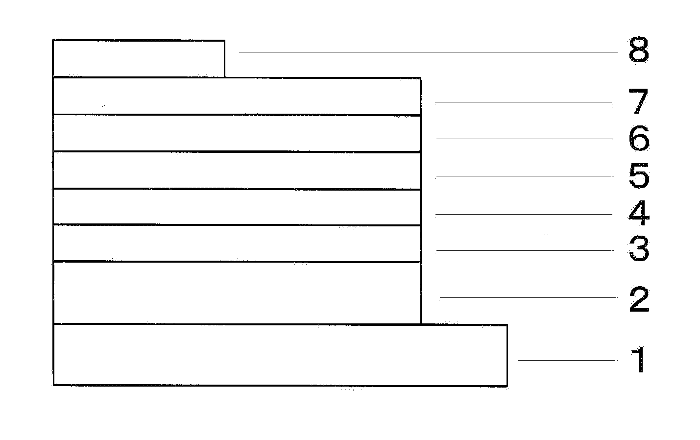
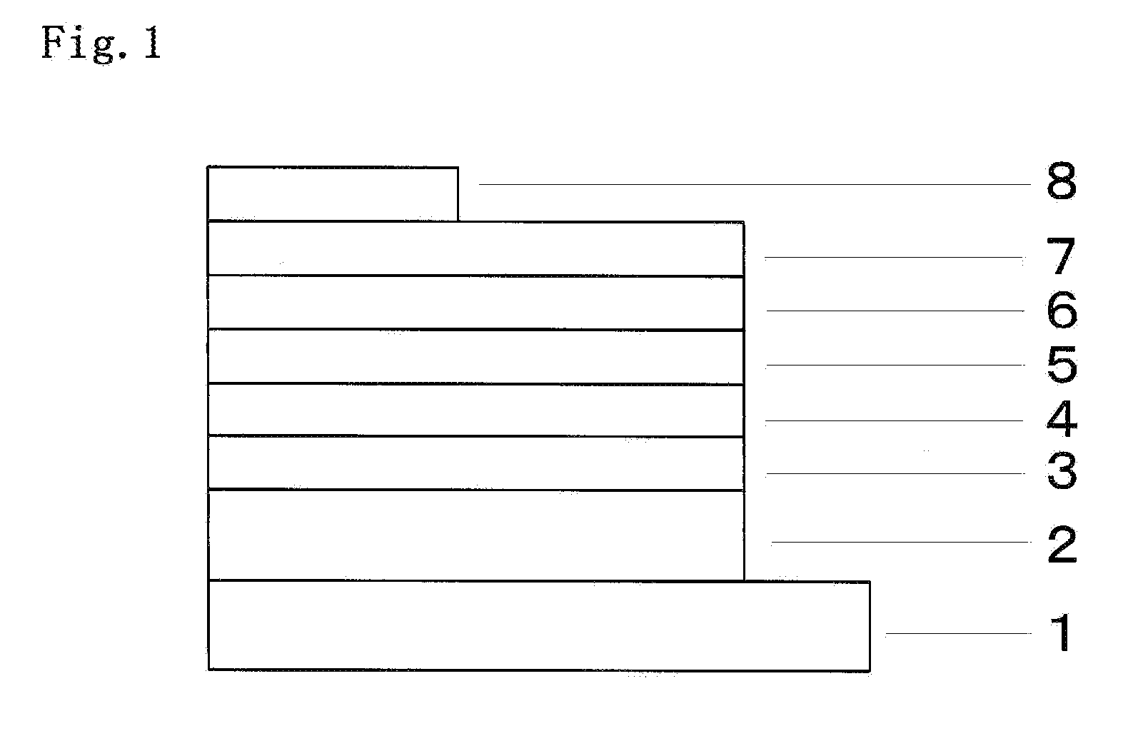
[0109]Each thin film was stacked by a vacuum deposition method at a degree of vacuum of 4.0×10⁻⁴ Pa on a glass substrate on which an anode formed of ITO having a thickness of 150 nm had been formed. First, copper phthalocyanine (CuPC) was formed into a hole-injecting layer having a thickness of 20 nm on the ITO. Next, 4,4-bis[N-(1-naphthyl)-N-phenylamino]biphenyl (NPB) was formed into a hole-transporting layer having a thickness of 20 nm. Next, Compound 1-2 as a first host, Compound 3-87 as a second host, and tris(2-phenylpyridine)iridium(III) (Ir(PPy)3) as a light-emitting layer guest were co-deposited from vapor deposition sources different from one another to form a light-emitting layer having a thickness of 30 nm. At this time, a vapor deposition rate ratio among the first host, the second host, and Ir(PPy)3 (volume rate ratio among vaporized products) was 47:47:6. Next, aluminum(III) bis(2-methyl-8-quinolinato)4-phenylphenolate (BAlq) was formed into a hole-blocking layer havin...

examples 2 to 4

[0111]Organic EL elements were each produced in the same manner as in Example 1 except that in Example 1, a compound shown in Table 1 was used as the light-emitting layer second host. An external power source was connected to each of the resultant organic EL elements and a DC voltage was applied to the element. As a result, an emission spectrum having a local maximum wavelength of 517 nm was observed for each of the organic EL elements and hence it was found that light emission from Ir(PPy)3 was obtained. The luminance, external quantum efficiency, and luminance half lifetime of each of the produced organic EL elements are shown in Table 1.

example 5

[0119]Each thin film was stacked by a vacuum deposition method at a degree of vacuum of 4.0×10⁻⁴ Pa on a glass substrate on which an anode formed of ITO having a thickness of 150 nm had been formed. First, CuPC was formed into a hole-injecting layer having a thickness of 25 nm on the ITO. Next, NPB was formed into a first hole-transporting layer having a thickness of 10 nm, and 4,4′,4″-tris(N-carbazolyl)-triphenylamine (TCTA) was formed into a second hole-transporting layer having a thickness of 10 nm. Next, Compound 1-114 as a first host, Compound 3-87 as a second host, and tris[1-14′-cyanophenyl)-3-methylbenzimidazol-2-ylidene-C2,C2′]-iridium(III) (Ir(cn-pmic)3) as a light-emitting layer guest were co-deposited from vapor deposition sources different from one another to form a light-emitting layer having a thickness of 30 nm. At this time, a vapor deposition rate ratio among the first host, the second host, and Ir(cn-pmic)3 was 45:45:10. Next, 2,9-dimethyl-4,7-diphenyl-1,10-phenan...


PUM

PropertyMeasurementUnit
ionization potentialaaaaaaaaaa
visible light transmittanceaaaaaaaaaa

Abstract

Provided is a practically useful organic EL element having high efficiency and high driving stability while being capable of being driven at a low voltage. The organic EL element has a light-emitting layer and any other organic layer between an anode and a cathode opposite to each other. The light-emitting layer contains at least two host materials and at least one light-emitting dopant. At least one of the host materials is a host material selected from compounds each having one or two indolocarbazole skeletons, and at least one of the other host materials is a host material selected from carbazole compounds each substituted with a dibenzofuran or a dibenzothiophene.

Description

TECHNICAL FIELD[0001]The present invention relates to an organic electroluminescent element (hereinafter referred to as “organic EL element”).BACKGROUND ART[0002]In general, an organic EL element includes a light-emitting layer and a pair of counter electrodes interposing the light-emitting layer therebetween in its simplest structure. That is, the organic EL element uses the phenomenon that, when an electric field is applied between both the electrodes, electrons are injected from a cathode and holes are injected from an anode, and each electron and each hole recombine in the light-emitting layer to emit light as energy.[0003]In recent years, progress has been made in developing an organic EL element using an organic thin film. In particular, development has been made to enhance luminous efficiency. In the course of the development, the efficiency of injection of carriers from the electrodes has been improved through the optimization of the kind of electrodes. In addition, there ha...

Claims


Application Information

Patent Timeline
Patent Type & Authority Applications(United States)
IPC IPC(8): H01L51/00H01L51/50H01L51/52C09K11/06
CPCH01L51/0067C09K11/06H01L51/0072H01L51/0073H01L51/0074H01L51/0068H01L51/0085H01L51/504H01L51/5278C09K2211/185H01L51/5016H01L2251/5384C07D405/14C07D409/14C07D487/04C09K2211/1029H10K85/654H10K85/6576H10K85/6574H10K85/6572H10K85/342H10K50/11H10K2101/10H10K2101/90H10K50/13H10K50/19H10K85/655
Inventor TADA, MASASHIKAI, TAKAHIRONOGUCHI, KATSUHIDETAKAHASHI, YASUHIROTERAO, YUHKITSUJI, TAISHINAKAJIMA, YUSUKEYUKI, TOSHINAO
Owner PIONEER CORP
Why Eureka
Try Eureka