Method of making a semiconductor device having a multicomponent oxide

a semiconductor device and multi-component technology, applied in the direction of semiconductor devices, electrical devices, transistors, etc., can solve the problems of difficult to accurately render motion and relatively slow switching speed of thin-film transistors

Active Publication Date: 2010-06-08
HEWLETT PACKARD DEV CO LP
View PDF22 Cites 232 Cited by
  • Summary
  • Abstract
  • Description
  • Claims
  • Application Information

AI Technical Summary

Problems solved by technology

Some types of thin-film transistors have relatively slow switching speeds because of low carrier mobility.
In some applications, such

Method used


Image

  • Method of making a semiconductor device having a multicomponent oxide
  • Method of making a semiconductor device having a multicomponent oxide
  • Method of making a semiconductor device having a multicomponent oxide

Examples


Embodiment Construction

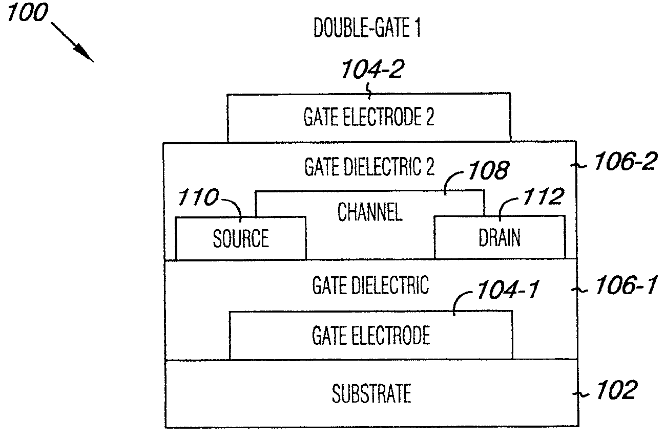
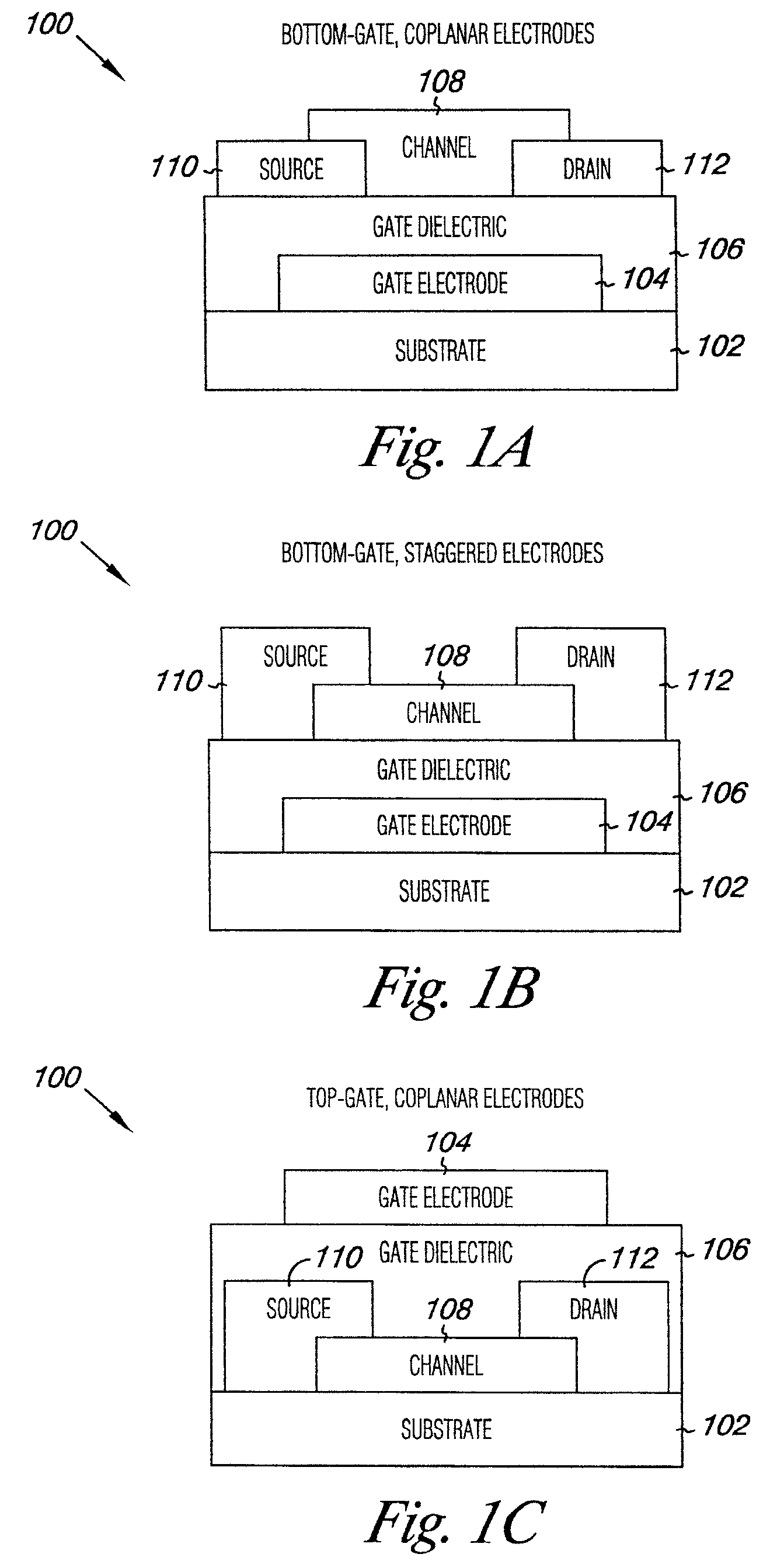
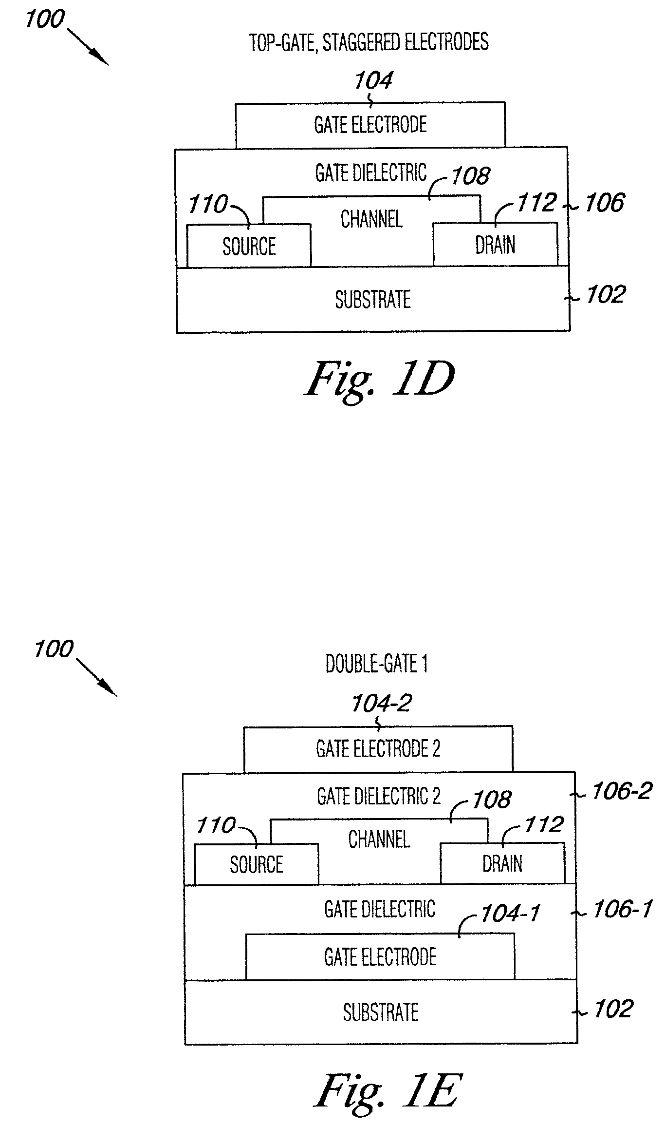
[0007]The exemplary embodiments of the present disclosure include semiconductor devices, such as transistors, that contain multicomponent oxide semiconductors. Additionally, exemplary embodiments of the present disclosure account for the properties possessed by transistors that contain multicomponent oxide semiconductors, e.g. optical transparency, and electrical performance. Exemplary embodiments include semiconductor devices having multicomponent oxide semiconductor structures that include at least one metal cation from group 12 and at least one metal cation from group 13 to form at least one of a three-component oxide, a four-component oxide, and a two-component oxide that includes zinc-gallium oxide, cadmium-gallium oxide, and cadmium-indium oxide. In some of the exemplary embodiments, the multicomponent oxide semiconductor structure can include an amorphous form, a single-phase crystalline state, or a mixed-phase crystalline state. As used herein, the terms multicomponent oxide...


PUM

PropertyMeasurementUnit
Transparencyaaaaaaaaaa

Abstract

One exemplary embodiment includes a semiconductor device. The semiconductor device can include a channel including one or more of a metal oxide including zinc-gallium, cadmium-gallium, cadmium-indium.

Description

[0001]This application is a divisional of Ser. No. 10 / 799,811 filed Mar. 12, 2004, now U.S. Pat. No. 7,297,977, which is hereby incorporated by reference.INTRODUCTION[0002]Semiconductor devices are used in a variety of electronic devices. For example, thin-film transistor technology can be used in liquid crystal display (LCD) screens. Some types of thin-film transistors have relatively slow switching speeds because of low carrier mobility. In some applications, such as LCD screens, use of thin-film transistors with relatively slow switching speeds can make it difficult to accurately render motion.BRIEF DESCRIPTION OF THE DRAWINGS[0003]FIGS. 1A-1F illustrate various embodiments of a semiconductor device, such as a thin-film transistor.[0004]FIG. 2 illustrates a cross-sectional schematic of an embodiment of a thin-film transistor.[0005]FIG. 3 illustrates a method embodiment for manufacturing an embodiment of a thin-film transistor.[0006]FIG. 4 illustrates an embodiment of an active ma...

Claims


Application Information

Patent Timeline
IPC IPC(8): H01L21/00H01L29/786
CPCH01L29/7869H01L29/78648Y10T408/5633
Inventor HOFFMAN, RANDY L.HERMAN, GREGORY S.MARDILOVICH, PETER P.
Owner HEWLETT PACKARD DEV CO LP
Why Eureka
Try Eureka