Semiconductor testing device and method of testing semiconductor memory

a technology of semiconductor memory and testing device, which is applied in the direction of information storage, static storage, digital storage, etc., can solve the problems of increasing data read/write time, and increasing data compression time, so as to reduce the compression time of pass/fail data

Inactive Publication Date: 2010-06-08
ADVANTEST CORP
View PDF8 Cites 6 Cited by
  • Summary
  • Abstract
  • Description
  • Claims
  • Application Information

AI Technical Summary

Benefits of technology

[0028]The present invention can provide a semiconductor testing device realizing reduction in compression time of pass / fail data of a device at a wafer process stage at the time of generating a wafer fail bitmap.

Problems solved by technology

In recent years, as the packing density of a semiconductor memory increases, various problems occur in the semiconductor memory.
However, as the capacity of a semiconductor memory increases, the data compression time is becoming longer.
A problem arises such that the period since data is read from the AFM until compressed data is stored in the CFBM is becoming longer.

Method used


Image

  • Semiconductor testing device and method of testing semiconductor memory
  • Semiconductor testing device and method of testing semiconductor memory
  • Semiconductor testing device and method of testing semiconductor memory

Examples


Embodiment Construction

[0033]The present invention will be described hereinbelow by using an embodiment of the invention. The embodiment does not limit the present invention in the scope of claims, and all of combinations of features described in the embodiment are not always necessary for the solving means of the present invention.

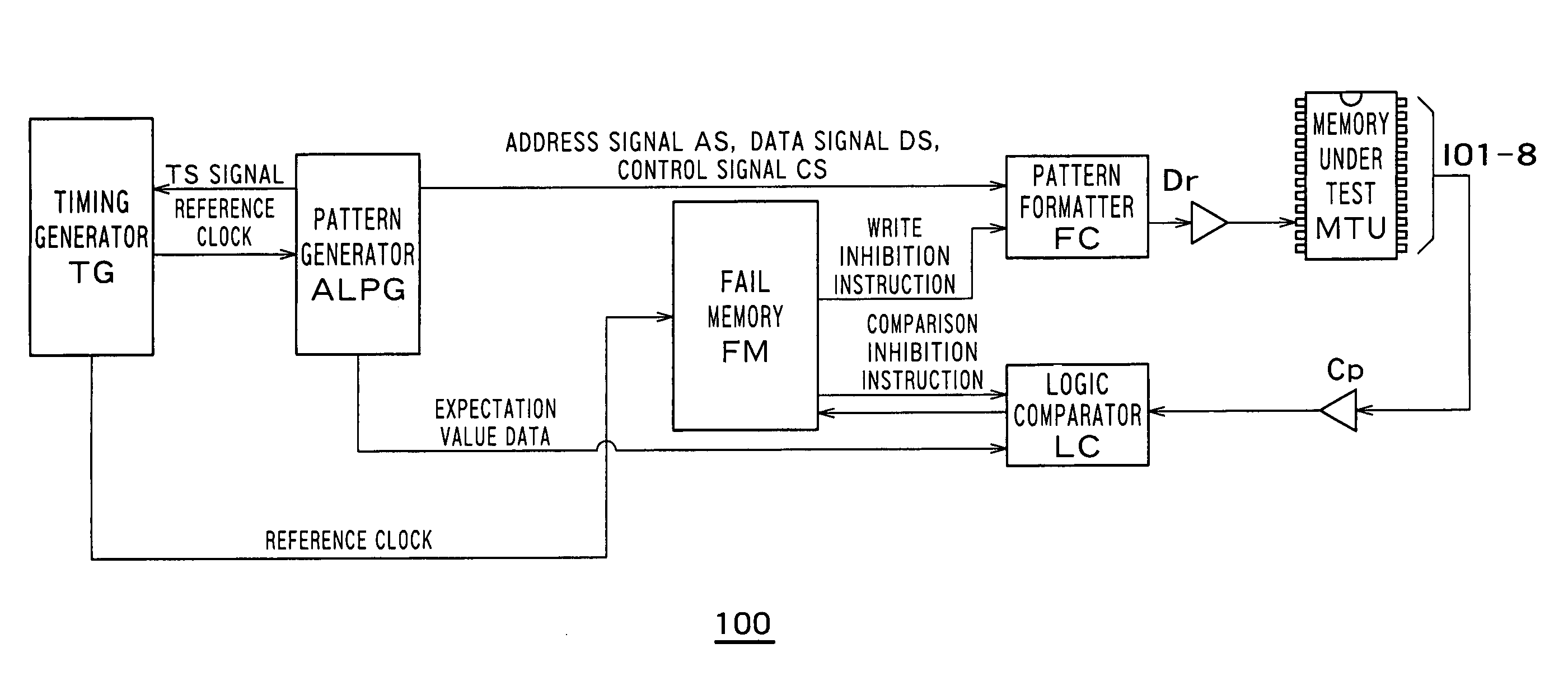
[0034]FIG. 1 is a block diagram of a semiconductor testing device 100 (hereinbelow, device 100) of the embodiment of the invention.

[0035]The device 100 has a timing generator TG, a pattern generator ALPG, a pattern formatter FC, a logic comparator LC, and a failure buffer memory FM. The pattern generator ALPG outputs a timing set signal (TS signal) to the timing generator TG. The timing generator TG receives the TS signal and generates timing edges of a number of various channels specified on the basis of timing sets described in a device test program. With the timing edge, the timing generator TG generates a reference clock. The pattern generator ALPG generates address informa...


PUM


Abstract

The disclosure concerns a semiconductor tester for testing a MUT, comprising a pattern generator; a pattern formatter; a comparator comparing a result signal from the MUT with an expectation value; a bad block memory; an AFM pre-storing pass / fail information of each of memory cells; a data compressor compressing data of pass / fail information in the AFM; a compression failure buffer memory storing data compressed; a good block register storing an address number of a good block prepared; and an address generator, wherein when the block to be compressed is a good one, the good block register sends a address number of the good block to the compress failure buffer memory.

Description

BACKGROUND OF THE INVENTION[0001]1. Field of the Invention[0002]The present invention relates to a semiconductor testing device and, for example, to a semiconductor testing device for testing a memory of a data storage type the quality of which is controlled blockwise if a device is good or not such as a NAND-type flash memory.[0003]2. Related Art[0004]A semiconductor memory testing device has a timing generator, a pattern generator, a pattern formatter, and a logic comparator. The timing generator generates a reference clock from timing data designated by a timing set signal (hereinbelow, called TS signal) output from the pattern generator. The pattern generator outputs test pattern data to be given to a memory under test (MUT) synchronously with the reference clock from the timing generator. The test pattern data is given to the pattern formatter. The pattern formatter shapes the test pattern data to a waveform of a timing necessary for a test, and applies the shaped test signal t...

Claims


Application Information

Patent Timeline
Patent Type & Authority Patents(United States)
IPC IPC(8): G11C7/00
CPCG11C29/56G11C29/56004G11C29/56008G11C2029/5606G11C2029/1208G11C2029/5604G11C8/04G11C29/00
Inventor TABATA, MAKOTO
Owner ADVANTEST CORP
Why Eureka
Try Eureka