Display methods and apparatus

a technology of display method and apparatus, applied in the field of image display, can solve the problems that backlit displays using mechanical light modulators have not yet demonstrated sufficiently attractive combinations of brightness and low power, and achieve the effects of reducing the power needed to operate a display, improving power management, and increasing capacitan

Active Publication Date: 2010-06-22
SNAPTRACK
View PDF427 Cites 35 Cited by
  • Summary
  • Abstract
  • Description
  • Claims
  • Application Information

AI Technical Summary

Benefits of technology

[0004]The power needed to operate a display can be reduced, in part, by taking advantage of asymmetries in capacitance of various elements in the display. The display includes an array of pixels. In particular, each pixel in the display includes at least one actuator, which has two electrodes. One electrode has a higher capacitance than the other. In addition, of the signals used to address and actuate the pixels in the display, some signals experience larger swings in voltage magnitude than other signals and some signals are switched more frequently than others. Driving these higher-magnitude or higher-frequency voltages on the lower capacitance electrode of each pixel improves power management.
[0005]More particularly, in one aspect, the invention relates to a display apparatus that includes a shutter assembly and a control matrix. The shutter assembly includes a shutter and a drive electrode. The shutter assembly and drive electrode have significantly different capacitances. The shutter assembly is configures such that in response to the generation of a potential difference between the shutter and the drive electrode, the shutter is electrostatically drawn towards the drive electrode. In one embodiment, the shutter assembly includes a mechanical support for substantially limiting the range of motion of the shutter to a plane parallel to a substrate upon which the shutter assembly is constructed.
[0009]In another embodiment, the shutter assembly includes a second drive electrode connected to a third voltage interconnect. Application of the first voltage to the first drive electrode results in the shutter assembly moving the shutter to an open position and application of a third voltage to the second drive electrode closes the shutter. Application of the second voltage, in one embodiment, however, prevents shutter movement.

Problems solved by technology

Backlit displays using mechanical light modulators have not yet demonstrated sufficiently attractive combinations of brightness and low power.

Method used


Image

  • Display methods and apparatus
  • Display methods and apparatus
  • Display methods and apparatus

Examples


Embodiment Construction

[0033]To provide an overall understanding of the invention, certain illustrative embodiments will now be described, including apparatus and methods for displaying images. However, it will be understood by one of ordinary skill in the art that the systems and methods described herein may be adapted and modified as is appropriate for the application being addressed and that the systems and methods described herein may be employed in other suitable applications, and that such other additions and modifications will not depart from the scope hereof.

[0034]This application is related to, and incorporates herein by reference, U.S. patent application Ser. No. 11 / 218,690, filed Sep. 2, 2005, U.S. patent application Ser. No. 11 / 251,035, filed Oct. 14, 2005, U.S. patent application Ser. No. 11 / 251,452, filed Oct. 14, 2005, and U.S. patent application Ser. No. 11 / 251,034, filed Oct. 14, 2005, the disclosures of which are herein incorporated by reference.

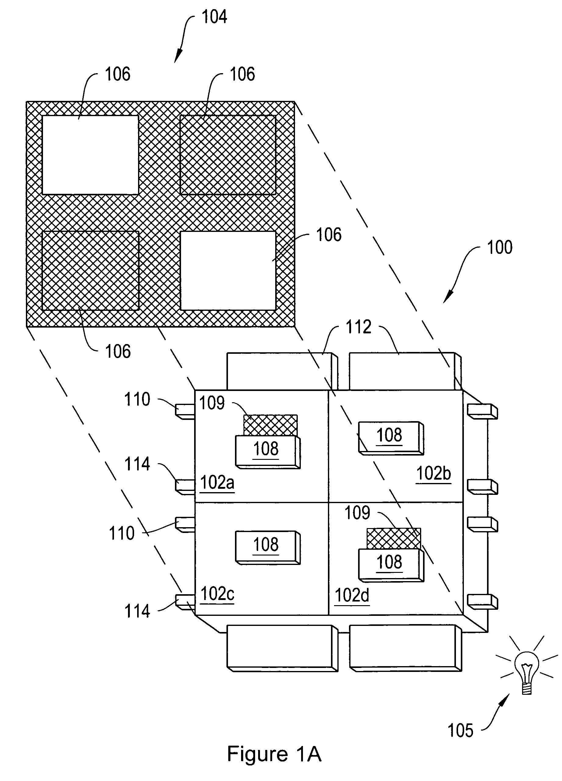
[0035]FIG. 1A is an isometric view of a di...


PUM


Abstract

The invention relates to methods and apparatus for forming images on a display utilizing a control matrix to control the movement of MEMs-based light modulators.

Description

CROSS-REFERENCE TO RELATED APPLICATIONS[0001]The instant application claims priority from provisional application No. 60 / 655,827, filed Feb. 23, 2005 and provisional application No. 60 / 676,053, filed Apr. 29, 2005, the disclosures of which are incorporated herein by reference in their entirety.FIELD OF THE INVENTION[0002]In general, the invention relates to the field of imaging displays, in particular, the invention relates to circuits for controlling light modulators incorporated into imaging displays.BACKGROUND OF THE INVENTION[0003]Displays built from mechanical light modulators are an attractive alternative to displays based on liquid crystal technology. Mechanical light modulators are fast enough to display video content with good viewing angles and with a wide range of color and grey scale. Mechanical light modulators have been successful in projection display applications. Backlit displays using mechanical light modulators have not yet demonstrated sufficiently attractive com...

Claims


Application Information

Patent Timeline
Patent Type & Authority Patents(United States)
IPC IPC(8): G09G3/18
CPCG02B26/04G09G3/346G09G2310/0262G09G2300/0842G09G2300/088G09G2300/08
Inventor HAGOOD, NESBITT W.MCALLISTER, ABRAHAMLEWIS, STEPHENBARTON, ROGER
Owner SNAPTRACK
Why Eureka
Try Eureka