
Compact solid-state laser with nonlinear frequency conversion using periodically poled materials

a solid-state laser and periodic pole technology, applied in semiconductor lasers, laser details, instruments, etc., can solve the problems of achieving wavelengths >470 nm in an efficient and reliable way, and affecting the efficiency and reliability of lasers

Inactive Publication Date: 2010-06-22
OOO SPECTRALUS
View PDF7 Cites 18 Cited by
  • Summary
  • Abstract
  • Description
  • Claims
  • Application Information

AI Technical Summary

Problems solved by technology

Efficient operation down to ˜650 nm (red color) can be achieved without serious technological challenges and some semiconductor laser designs can be extended down to ˜635 nm with however decreasing efficiency and reliability.
However, achieving wavelengths >470 nm in an efficient and reliable way represents a nearly insurmountable challenge.
Thus, the majority of the visible spectrum (i.e., from ˜470 nm blue to ˜635 nm red) does not currently have an efficient semiconductor laser solution.
Indeed, no direct solution for a green semiconductor laser is currently available.
However, the currently available microchip lasers lack the efficiency and flexibility required in many applications, especially at higher power levels, e.g. from several hundred milliwatts up to several Watts.
This is mainly due to the frequency conversion inefficiency of conventional nonlinear materials such as KTP.
Furthermore, traditional bulk nonlinear materials such as KTP are restricted as to their scope of frequency conversion.
For example, KTP is used for frequency doubling into the green color but cannot be practically used for frequency doubling into the blue color, so one has to search for different nonlinear materials with their own limitations in efficiency, reliability, and cost.
However, embodiments of that invention suffer from serious limitations, which, to our knowledge, have prevented commercialization of this platform, and, to this day, visible wavelength microchip lasers continue to rely on bulk nonlinear materials such as KTP and KNbO3, the latter material being used to produce the blue color (see, e.g., World Patent Application WO2005 / 036,703).
However, the practical use of these materials is very limited.
Like bulk KTP, periodically poled KTP can only perform well at low power levels (a few milliwatts or possibly even tens of milliwatts in the visible) but suffers from passive and induced absorption (“gray tracking”) at higher power levels.
In addition, KTP crystal production is not easily scalable to mass production quantities at low cost as is required by some applications such as consumer-electronics displays.
LiNbO3 and LiTaO3 are scalable to high-volume production and can be readily periodically poled, but suffer from visible-light-induced degradation (“photo-refractive damage”) that makes it impossible to use these crystals to produce even milliwatts of visible light without severe degradation.
However, this requires using ovens for maintaining the nonlinear crystals at a high-temperature.
Such ovens are incompatible with a low-cost, efficient laser fabrication, especially in a microchip geometry.
Thus, the laser designs described by Laurell, cannot be implemented in a high-power, low-cost, compact, and efficient architecture.
The possible use of PPLN and PPKTP is mentioned but it is not taught how one can overcome the limitations of these crystals, especially their afore mentioned reliability limitations.
The high-temperature operation, mentioned above, partially solves the problem, but is not suitable for most applications.
However, none of the prior art workers have taught a means of achieving a high output power, stable ambient temperature operable frequency doubled laser suitable for producing green and blue light in a low-cost, mass-manufacturable design.
In short, known technical approaches cannot provide a reliable, cost-effective, and compact frequency converted laser.

Method used


Image

  • Compact solid-state laser with nonlinear frequency conversion using periodically poled materials
  • Compact solid-state laser with nonlinear frequency conversion using periodically poled materials
  • Compact solid-state laser with nonlinear frequency conversion using periodically poled materials

Examples


Embodiment Construction

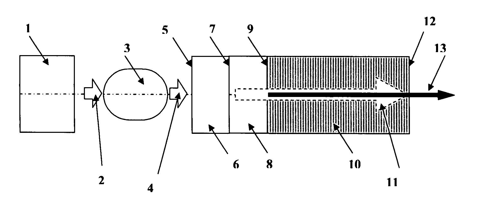
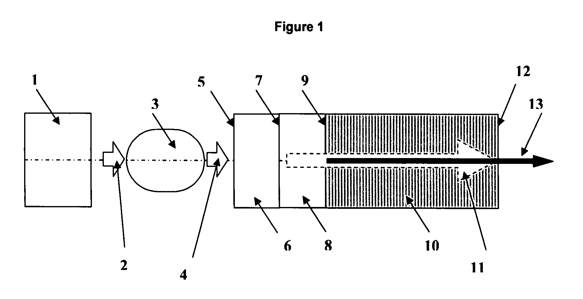
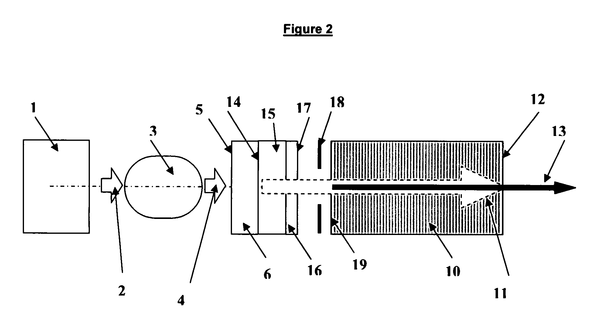
[0018]FIG. 1 illustrates a preferred embodiment of the present invention. The pump diode laser 1, emits a beam 2, for example, at a wavelength between 800 and 900 nm, such as ˜808 nm or 885 nm for efficient absorption by the gain material (element) 8. The beam 2 is frequently astigmatic and beam-shaping optics 3 are advantageously used to convert the pump beam 2 into the beam 4 so that the beam 4 forms a circular cross-section of the desired diameter on the surface 7 of gain medium 8. This type of pumping arrangement is known in the art and can efficiently overlap the pump area in the gain element with the intracavity circulating beam, which must be a single-spatial mode (or TEM00) for efficient nonlinear frequency doubling. A suitable diameter for the pump spot on the gain element 8 is in the range of 50 to 300 microns. The beam-shaping optics can be a micro-lens, a gradient-index lens, or a combination of such optical elements. When efficiency can be sacrificed in favor of simplic...


PUM


Abstract

A compact optically-pumped solid-state laser designed for efficient nonlinear intracavity frequency conversion into desired wavelengths using periodically poled nonlinear crystals. These crystals contain dopants such as MgO or ZnO and / or have a specified degree of stoichiometry that ensures high reliability. The laser includes a solid-state gain media chip, such as Nd:YVO4, which also provides polarization control of the laser; and a periodically poled nonlinear crystal chip such as PPMgOLN or PPZnOLT for efficient frequency doubling of the fundamental infrared laser beam into the visible wavelength range. The described designs are especially advantageous for obtaining low-cost green and blue laser sources.

Description

PRIORITY INFORMATION[0001]This application claims priority from, commonly assigned U.S. Provisional Application U.S. 60 / 795,212, filed Apr. 27, 2006.BACKGROUND OF THE INVENTION[0002]Compact, efficient, and low-cost laser sources in the visible and ultraviolet spectral regions have long been desired for a variety of applications. These applications include laser-based projection displays, optical storage, bio-analytical instrumentation, semiconductor inspection and spectroscopy. Semiconductor lasers, which provide a low-cost, compact, and efficient platform, rely on material systems such as InGa(AI)P that lase most efficiently in the near-infrared spectral region. Efficient operation down to ˜650 nm (red color) can be achieved without serious technological challenges and some semiconductor laser designs can be extended down to ˜635 nm with however decreasing efficiency and reliability. On the shorter wavelength side of the visible region, GaN systems have been developed in recent yea...

Claims


Application Information

Patent Timeline
Patent Type & Authority Patents(United States)
IPC IPC(8): H01S3/10
CPCH01S3/109G02F1/3558G02F1/3775G02F2203/11H01S3/08036H01S5/141H01S3/08054H01S3/1115H01S3/113H01S3/0805
Inventor ESSAIAN, STEPANSHCHEGROV, ANDREI
Owner OOO SPECTRALUS
Learn More