Polishing apparatus and polishing method

a polishing apparatus and polishing technology, applied in the direction of grinding machines, edge grinding machines, manufacturing tools, etc., can solve the problems of reducing the contact area of polishing tape with the wafer, affecting the polishing effect, etc., to achieve high speed

Active Publication Date: 2010-06-29
EBARA CORP +1
View PDF13 Cites 26 Cited by
  • Summary
  • Abstract
  • Description
  • Claims
  • Application Information

AI Technical Summary

Benefits of technology

[0005]The present invention has been made in view of the above drawbacks. It is, therefore, a first object of the present invention to provide a polishing apparatus and a polishing method which can uniformly polish a notch portion or the like of a substrate such as a semiconductor wafer at a high speed without scratches on the substrate due to polishing by a polishing tape.
[0006]According to a first aspect of the present invention, there is provided a polishing apparatus which can achieve uniform and high-speed polishing without scratches on a substrate due to polishing. The polishing apparatus has a polishing tape, a supply reel for supplying the polishing tape to a contact portion at which the polishing tape is brought into contact with a portion of a substrate to be polished, and a take-up reel for winding up the polishing tape from the contact portion. The polishing apparatus also has a first guide portion having a guide surface for guiding the polishing tape from the supply reel to supply the polishing tape directly to the contact portion, a second guide portion having a guide surface for guiding the polishing tape supplied directly from the contact portion to supply the polishing tape to the take-up reel, and a drive mechanism configured to move the polishing tape and the substrate relative to each other. At least one of the guide surface of the first guide portion and the guide surface of the second guide portion has a shape corresponding to a shape of the portion of the substrate to be polished.
[0007]According to a second aspect of the present invention, there is provided a polishing method which can achieve uniform and high-speed polishing without scratches on a substrate due to polishing. According to this polishing method, a polishing tape is supplied to a guide surface of a first guide portion. The polishing tape is supplied from the guide surface of the first guide portion directly to a contact portion at which the polishing tape is brought into contact with a portion of a substrate to be polished. The polishing tape is supplied from the contact portion directly to a guide surface of a second guide portion. A portion of the polishing tape is deformed so as to correspond to a shape of the portion of the substrate to be polished by at least one of the guide surface of the first guide portion and the guide surface of the second guide portion. The portion of the substrate to be polished and the polishing tape are moved relative to each other to polish the portion of the substrate.
[0009]According to the present invention, a polishing tape is deformed so as to correspond to a shape of a portion such as a notch portion of a semiconductor substrate before the portion of the semiconductor substrate is polished. Therefore, the polishing tape becomes likely to be brought into uniform contact with the entire portion of the substrate to be polished. Accordingly, the substrate becomes unlikely to be scratched due to polishing. Thus, uniform and high-speed polishing can be achieved.

Problems solved by technology

Accordingly, a wafer may be flawed or unevenly polished at the notch portion according to polishing conditions.
Further, if the polishing tape is insufficiently deformed, an area of the polishing tape contacting the wafer is reduced so that it is difficult to conduct stable polishing.
In this case, it is difficult to achieve uniform polishing.
Additionally, it is uneconomic in that the entire surface of the polishing tape is not used for polishing.
Accordingly, it takes much time to complete the polishing process.
Thus, if polishing conditions are improperly set when the notch portion of the wafer is polished, there arise problems such as scratches on the wafer by the edge portions of the polishing tape or unevenly polishing.
However, when a polishing tape is thinned, resistance to tension is reduced.
Thus, the polishing tape has a limitation of the thinness.

Method used


Image

  • Polishing apparatus and polishing method
  • Polishing apparatus and polishing method
  • Polishing apparatus and polishing method

Examples


first embodiment

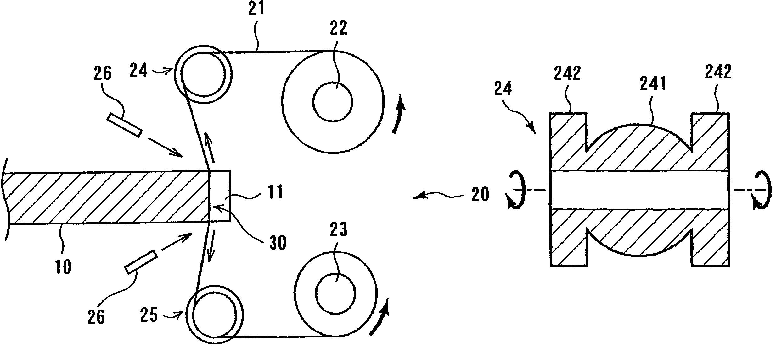
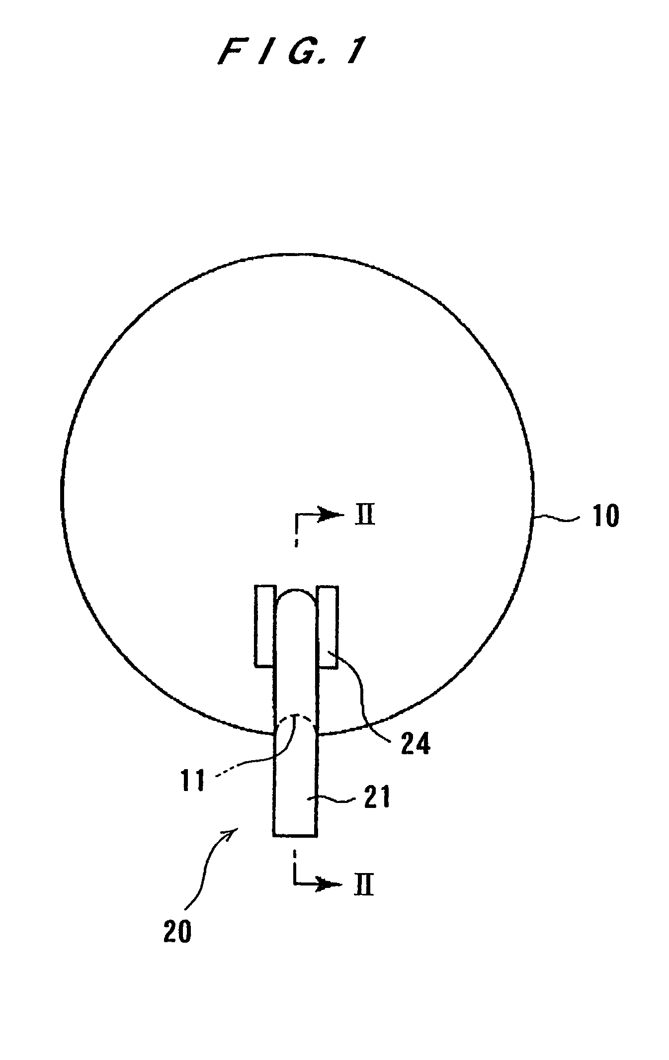
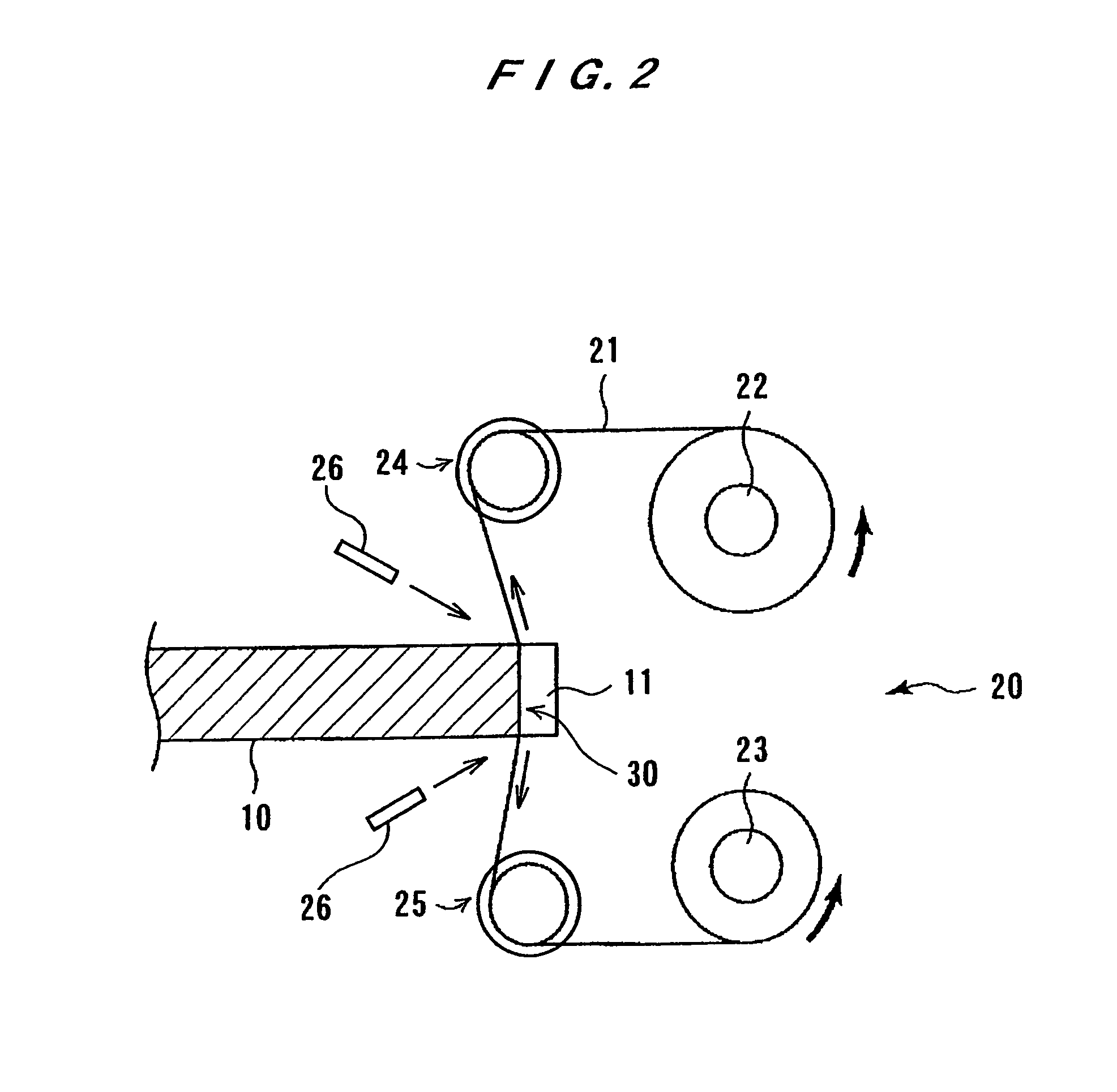
[0042]FIG. 1 is a plan view showing a polishing apparatus according to the present invention, and FIG. 2 is a cross-sectional view taken along line II-II of FIG. 1. The polishing apparatus in the present embodiment serves to polish a notch portion formed in a peripheral portion of a semiconductor wafer. The polishing apparatus has a polishing mechanism 20 for polishing a notch portion 11 of a semiconductor wafer 10 held horizontally on a stage (not shown).

[0043]As shown in FIGS. 1 and 2, the polishing mechanism 20 has a polishing tape 21 with abrasive particles, a supply reel 22 for supplying a polishing tape 21 to a contact portion 30, at which the polishing tape 21 is brought into contact with a portion of the wafer 10 to be polished, a take-up reel 23 for winding up the polishing tape 21 from the contact portion 30, a first guide portion (guide roller) 24 for guiding the polishing tape 21 from the supply reel 22 to supply the polishing tape 21 directly to the contact portion 30, ...

second embodiment

[0054]FIG. 7 is a plan view showing a polishing apparatus according to the present invention. The polishing apparatus in the present embodiment serves to polish a bevel portion at a peripheral portion of a wafer. The polishing apparatus has a polishing mechanism 50 for polishing a bevel portion 12 of a semiconductor wafer 10 held horizontally on a rotatable stage (not shown).

[0055]As shown in FIG. 7, the polishing mechanism 50 has a polishing tape 121 with abrasive particles, a supply reel 122 for supplying a polishing tape 121 to a contact portion 130, at which the polishing tape 121 is brought into contact with a portion of the wafer 10 to be polished, a take-up reel 123 for winding up the polishing tape 121 from the contact portion 130, a first guide portion 54 for guiding the polishing tape 121 from the supply reel 122 to supply the polishing tape 121 directly to the contact portion 130, a second guide portion (guide roller) 55 for guiding the polishing tape 121 supplied directl...

third embodiment

[0076]Further, polishing heads 581-585 as shown in FIGS. 18A through 18E may be employed as variations of the polishing heads in the In this example, angles of the polishing heads 581-585 are fixed, but angles of surfaces contacting the polishing tape 121 are varied in elastic members 591-595 of the respective polishing heads 581-585. Thus, the polishing tape 121 is pressed against the wafer 10 at respective predetermined angles. As described above, the surfaces of the elastic members 591-595 to press the polishing tape 121 against the wafer 10 are slopes. These elastic members 591-595 are attached to the polishing heads 581-585. Accordingly, it is possible to readily achieve polishing with a plurality of angles. Therefore, it is possible to dispense with the aforementioned mechanism for changing angles of the polishing heads.

[0077]FIG. 19 is a front view showing a first variation 20a of the polishing mechanism 20 in the first embodiment described above. The polishing mechanism 20a...


PUM

PropertyMeasurementUnit
widthaaaaaaaaaa
thicknessaaaaaaaaaa
speedaaaaaaaaaa

Abstract

A polishing apparatus has a polishing tape (21), a supply reel (22) for supplying the polishing tape (21) to a contact portion (30) at which the polishing tape (21) is brought into contact with a notch portion (11) of a substrate (10), and a take-up reel (23) for winding up the polishing tape (21) from the contact portion (30). The polishing apparatus also has a first guide portion (24) having as guide surface (241) for supplying the polishing tape (21) directly to the contact portion (30), and a second guide portion (25) having a guide surface for supplying the polishing tape (21) tot the take-up reel (23). The guide surface (241) of the first guide portion (24) and / or the guide surface of the second guide portion (25) has a shape corresponding to a shape of the notch portion (11) of the substrate (10).

Description

TECHNICAL FIELD[0001]The present invention relates to a polishing apparatus and a polishing method, and more particularly to a polishing apparatus and a polishing method to polish a substrate such as a semiconductor wafer by a polishing tape.BACKGROUND ART[0002]Heretofore, a polishing tape having abrasive particles has been employed to polish a notch portion formed in a semiconductor wafer. Specifically, a polishing tape is brought into contact with a notch portion of a semiconductor wafer and moved in a direction perpendicular to a surface of the wafer to polish the notch portion of the wafer.[0003]In this conventional method, a polishing tape is deformed along a notch portion of a wafer under a polishing load. Edge portions of the polishing tape may scratch the notch portion of the wafer according to polishing conditions. Accordingly, a wafer may be flawed or unevenly polished at the notch portion according to polishing conditions. Further, if the polishing tape is insufficiently ...

Claims


Application Information

Patent Timeline
Patent Type & Authority Patents(United States)
IPC IPC(8): B24B1/00
CPCB24B9/065H01L21/02021B24B21/002H01L21/304
Inventor KUBOTA, TAKEOSHIGETA, ATSUSHITOYOTA, GENTAKAHASHI, TAMAMIFUKUOKA, DAISAKUITO, KENYA
Owner EBARA CORP
Why Eureka
Try Eureka