Check patentability & draft patents in minutes with Patsnap Eureka AI!

Manufacturing method of group III nitride semiconductor light-emitting device

a nitride semiconductor and manufacturing method technology, applied in the direction of superimposed coating process, vacuum evaporation coating, coating, etc., can solve the problem of difficult epitaxial growth of crystals directly on the substrate, large lattice mismatch, and inability to obtain favorable crystals, etc., to achieve favorable crystallinity

Active Publication Date: 2010-07-06
TOYODA GOSEI CO LTD
View PDF11 Cites 4 Cited by
  • Summary
  • Abstract
  • Description
  • Claims
  • Application Information

AI Technical Summary

Benefits of technology

This method enables the deposition of group III nitride semiconductor layers with improved crystallinity and conductivity, suitable for high-performance light-emitting devices such as LEDs, by optimizing substrate temperature, gas ratios, and dopant incorporation, thereby overcoming previous limitations in sputtering techniques.

Problems solved by technology

Furthermore, they have a potential of offering characteristics that conventional III-V compound semiconductors cannot offer.
However, there is a large lattice mismatch between such a hetero-substrate and a group III nitride crystal that is epitaxially grown thereon.
In the presence of such a large lattice mismatch, it is difficult to epitaxially grow a crystal directly on a substrate.
Even if a crystal is grown, it is not possible to obtain a favorable crystal.
However, they are still expensive and no advantage is found for their industrial use.
However, with a substrate whose topmost surface is made from a group III nitride semiconductor, no case has been reported of a manufacture of a crystalline group III nitride semiconductor which is favorable enough to fabricate a device such as an LED with by the sputtering method.

Method used


Image

  • Manufacturing method of group III nitride semiconductor light-emitting device
  • Manufacturing method of group III nitride semiconductor light-emitting device
  • Manufacturing method of group III nitride semiconductor light-emitting device

Examples


example 1

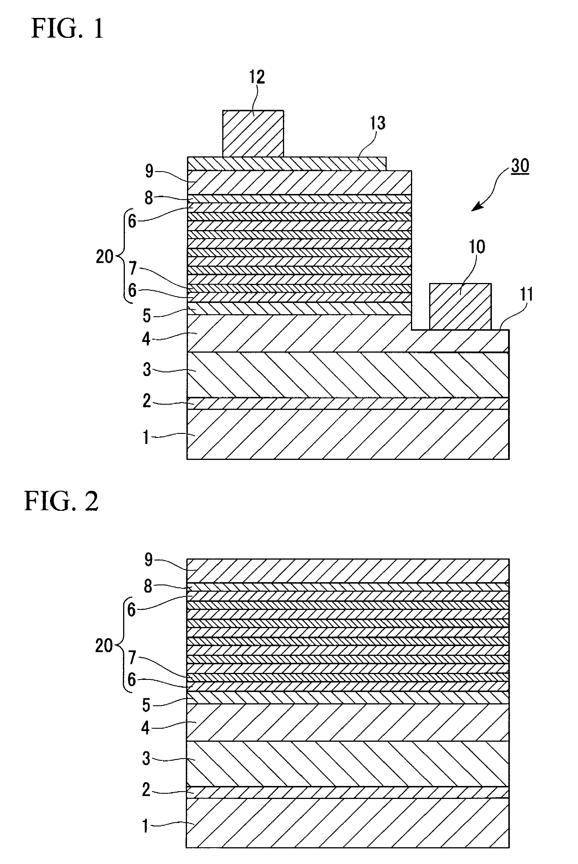
[0105]A (0001) c-plane sapphire substrate with a diameter of 2 inches whose surface was mirror-polished is cleaned with a hydrofluoric acid and an organic solvent, and was then introduced into a chamber of a sputtering apparatus. The sputtering apparatus had a mechanism which had a radio frequency power source and rotated a magnet in a sputtering target to thereby cause a magnetic field applied area to be shifted.

[0106][Substrate cleaning] Nitrogen gas was introduced into the chamber at a flow rate of 15 sccm, and then a substrate temperature was increased to 750° C. Furthermore, with an intrachamber pressure maintained at 0.08 Pa, a radio frequency bias at 50 W was applied to the substrate side while rotating a magnet in a sputtering target, to expose the substrate surface to N2 plasma. Thereby, the substrate was cleaned. After that, the plasma generation was stopped.

[0107][Buffer layer formation] Next, in addition to nitrogen gas, argon gas was newly introduced, and the substrate ...

example 2

[0115]In Example 2, a sample made of a buffer layer, a foundation layer, and an n-type contact layer was fabricated in the same condition as in Example 1, the exception being that Si doping was performed in forming the n-type contact layer. The Si doping was formed by the sputter deposition with an Si small piece being placed on the Ga sputtering target. The ratio of a surface area of the Si small piece to that of a Ga metal in the Ga sputtering target was approximately 0.2%.

[0116]A surface of the n-type contact layer of the sample obtained in Example 2 was specular and transparent. A Hall effect measurement on the n-type contact layer was performed, which showed n-type conductivity and a carrier concentration of 2×10¹⁸ / cm3. The results of Example 2 are shown in Table 2.

[0117]

TABLE 2Example 2gas atmosphereArgon gas flow10rate (sccm)Nitrogen gas flow10rate (sccm)gas flow ratio50%of N2 to ArHall effectconductivityn-typemeasurementcarrier concentration2 × 1018(unit: / cm3)crystallinitygo...

example 3

[0118]In Example 3, a sample made of a buffer layer, a foundation layer, and an n-type contact layer was fabricated similar to Example 2, the exception being that when the n-type contact layer was formed, a substrate temperature was 900° C. and that the intrachamber gas atmosphere had an argon gas flow rate of 5 sccm and a nitrogen gas flow rate of 15 sccm (the ratio of N2 to the whole gas being 75%).

[0119]A surface of the n-type contact layer of the sample obtained in Example 3 was specular and transparent. A Hall effect measurement on the n-type contact layer was performed. It showed n-type conductivity and a carrier concentration of 7×10⁹ / cm3.


PUM

PropertyMeasurementUnit
RF voltageaaaaaaaaaa
distanceaaaaaaaaaa
temperatureaaaaaaaaaa

Abstract

The present invention provides a manufacturing method of a group III nitride semiconductor light-emitting device, including a lamination step of forming a plurality of lamination films including a group III nitride semiconductor on a substrate, in which a substrate on which is formed a foundation layer including a monocrystalline group III nitride semiconductor is used as the substrate, and lamination films are formed on the foundation layer by a sputtering method, with the substrate including the foundation layer and a target made from a group III metal or an alloy including a group III metal being placed in a sputtering chamber.

Description

TECHNICAL FIELD[0001]The present invention relates to a manufacturing method of a group III nitride semiconductor represented by a general formula of AlaGabIncN (where 0≦a≦1, 0≦b≦1, 0≦c≦1, a+b+c=1), more particularly to a manufacturing method of a group III nitride semiconductor light-emitting device in the case of depositing a crystalline film with the same composition of that of the topmost surface.[0002]Priority is claimed on Japanese Patent Application No. 2007-121541, filed on May 2, 2007, the contents of which are incorporated herein by reference.BACKGROUND ART[0003]Group III nitride semiconductors have a direct transition band gap with energy corresponding to that from the visible light region to the ultraviolet light region, and hence are capable of light emission with high efficiency. Therefore, commercialized products using the semiconductor light-emitting device such as a light-emitting diode (hereinafter referred to as LED) or a laser diode (hereinafter referred to as LD...

Claims


Application Information

Patent Timeline
Patent Type & Authority Patents(United States)
IPC IPC(8): H01L21/00H01L21/31C23C14/34H01L33/00
CPCC23C14/0036C23C14/06C23C14/0641C23C28/42H01L33/007C23C28/04H01L21/0237H01L21/02458H01L21/0262H01L21/02631H01L21/0254
Inventor MIKI, HISAYUKISASAKI, YASUMASA
Owner TOYODA GOSEI CO LTD
Features
  • R&D
  • Intellectual Property
  • Life Sciences
  • Materials
  • Tech Scout
  • Unparalleled Data Quality
  • Higher Quality Content
  • 60% Fewer Hallucinations
Learn More