Ion implanter and method for implanting a wafer

a technology of implanter and wafer, which is applied in the direction of beam deviation/focusing by electric/magnetic means, instruments, and therapy, etc., can solve the problems of uniform etching of uniform doping results over the wafer, non-uniform net result formation in the wafer, and non-uniform deposited layer of uniform doping results, etc., to achieve the effect of offs

Active Publication Date: 2010-07-06
ADVANCED ION BEAM TECHNOLOGY INC
View PDF4 Cites 14 Cited by
  • Summary
  • Abstract
  • Description
  • Claims
  • Application Information

AI Technical Summary

Benefits of technology

[0010]The invention can be applied to offset the non-uniformity of the former and / or latter process of a semiconductor manufacturing process. Whenever the non-uniformity of the former and / or latter process can be essentially measured and / or estimated, how to offset the non-uniformity by non-uniformly etch process also can be essentially calculated and / or estimated. Hence, by using the method and ion implanter proposed by the invention to simply adjust the non-uniformity of etching process, all these non-uniformities can be effectively offset and then net result of semiconductor manufacturing process can be essentially uniform.

Problems solved by technology

Hence, even the ion implantation process can uniformly implant the wafer, the net result formed in the wafer may be non-uniform if at least one latter process or former process has a non-uniform result.
For example, an etching process after the ion implantation may non-uniformly etch the wafer, such that the uniform doping result is non-uniformly etched over the wafer.
In addition, a depositing process before the ion implantation may deposit a layer with a non-uniform thickness, such that the uniform doping result is formed on a non-uniform deposited layer.
Therefore, the net result of both the implanting process and the former / latter process may be non-uniformity.
However, the cost and the difficulty may be very high, especially some specific former / latter processes are very difficult to achieve a high uniform result.
Clearly, the additional mask can blank a specific portion of the wafer and only allow other portions of the wafer to be implanted.
However, the manufacturing cost due to the usage of additional masks is high.

Method used


Image

  • Ion implanter and method for implanting a wafer
  • Ion implanter and method for implanting a wafer
  • Ion implanter and method for implanting a wafer

Examples


Embodiment Construction

[0021]Reference will now be made in detail to specific embodiments of the present invention. Examples of these embodiments are illustrated in the accompanying drawings. While the invention will be described in conjunction with these specific embodiments, it will be understood that it is not intended to limit the invention to these embodiments. In fact, it is intended to cover alternatives, modifications, and equivalents as may be included within the spirit and scope of the invention as defined by the appended claims. In the following description, numerous specific details are set forth in order to provide a through understanding of the present invention. The present invention may be practiced without some or all of these specific details. In other instances, well-known process operations are not described in detail in order not to obscure the present invention.

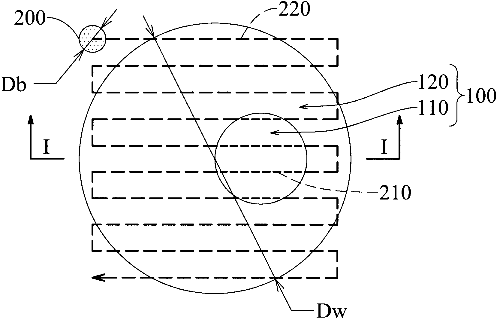
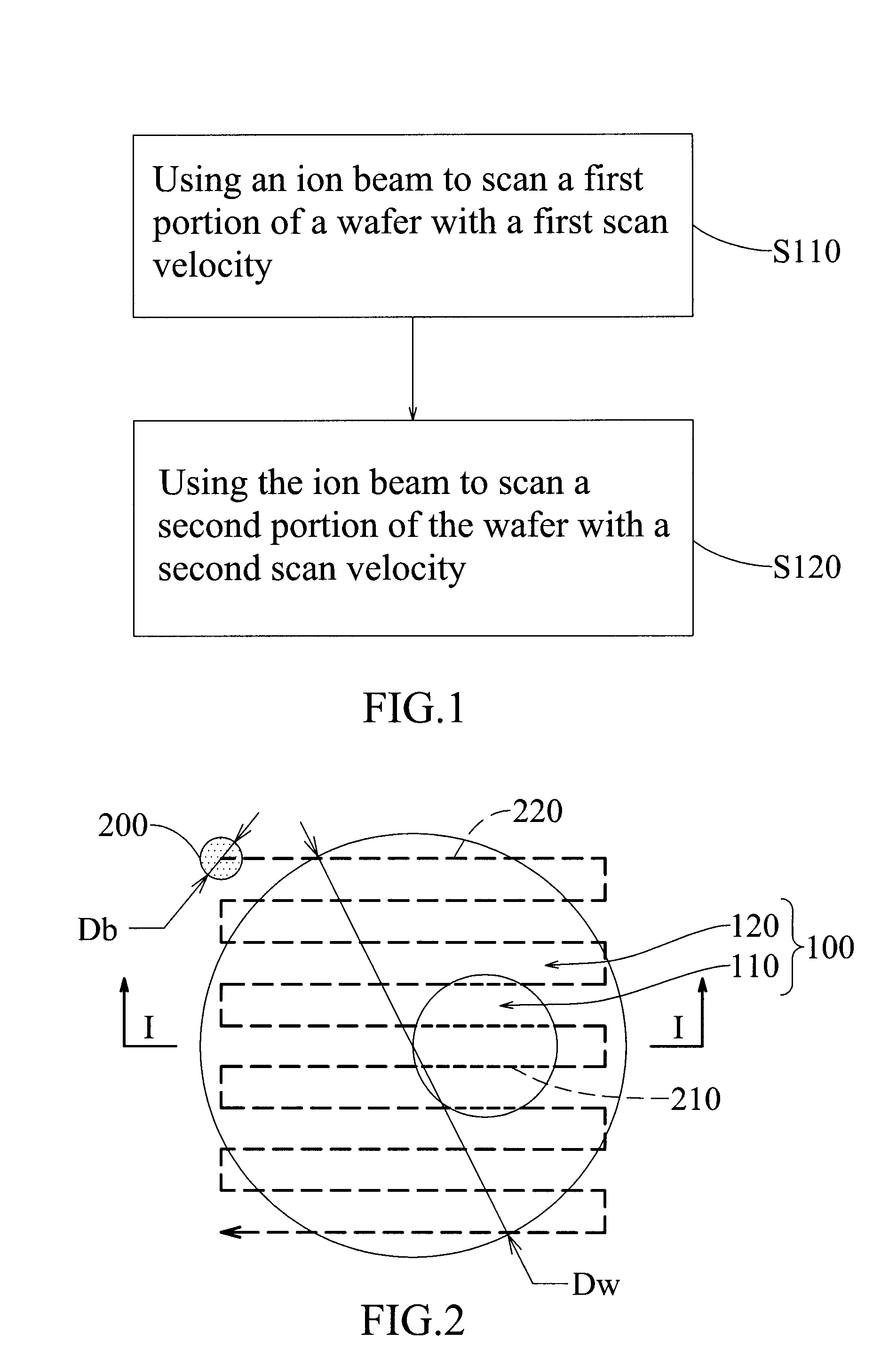
[0022]FIG. 1 illustrates a flow chart of a method for implanting a wafer according to an embodiment of the present invention...


PUM


Abstract

An ion implanter and a method for implanting a wafer are provided, wherein the method includes the following steps. First, a wafer has at least a first portion requiring a first doping density and a second portion requiring a second doping density is provided. The first doping density is larger than the second doping density. Thereafter, the first portion is scanned by an ion beam with a first scanning parameter value, and the second portion is scanned by the ion beam with a second scanning parameter value. The first scanning parameter value can be a first scan velocity, and the second scanning parameter value can be a second scan velocity different than the first scan velocity. Alternatively, the first scanning parameter value can be a first beam current, and the second scanning parameter value can be a second beam current different than the first beam current.

Description

FIELD OF THE INVENTION[0001]The present invention generally relates to an ion implanter and a method for implanting a wafer, and more particularly to an ion implanter and a method which may offset a non-uniformity of a former or latter process by implanting different portions of the wafer with different doping densities.DESCRIPTION OF THE RELATED ART[0002]Ion implantation process is an implanting process used in semiconductor manufacturing technology. In ion implantation process, an ion beam with a fixed ion beam current is used to scan through a wafer with a fixed velocity for uniformly implanting ions into the wafer. However, there are many processes in the semiconductor manufacturing technology. Hence, even the ion implantation process can uniformly implant the wafer, the net result formed in the wafer may be non-uniform if at least one latter process or former process has a non-uniform result. For example, an etching process after the ion implantation may non-uniformly etch the ...

Claims


Application Information

Patent Timeline
Patent Type & Authority Patents(United States)
IPC IPC(8): H01J37/317H01J37/08H01L21/265
CPCH01J37/3023H01J37/3172H01J2237/043H01J2237/045H01J2237/30461H01J2237/30477H01J2237/30483
Inventor WAN, ZHIMINSHEN, CHENG-HUIJEN, KO-CHUAN
Owner ADVANCED ION BEAM TECHNOLOGY INC
Why Eureka
Try Eureka