Semiconductor substrate, method for manufacturing semiconductor substrate, semiconductor device, and electronic device

a semiconductor substrate and semiconductor technology, applied in the direction of semiconductor/solid-state device manufacturing, basic electric elements, electric devices, etc., can solve the problem that the problem of ion irradiation cannot be avoided

Inactive Publication Date: 2010-07-27
SEMICON ENERGY LAB CO LTD
View PDF28 Cites 19 Cited by
  • Summary
  • Abstract
  • Description
  • Claims
  • Application Information

AI Technical Summary

Benefits of technology

[0010]In the present invention, plasma treatment is performed to the surface of a single crystal semiconductor layer after ion irradiation. Accordingly, contaminant on the surface of the single crystal semiconductor layer can be removed and the minute surface can be formed. In other words, a defect in an interface between the single crystal semiconductor layer and an insulating layer to be formed later can be reduced.

Problems solved by technology

However, as for the problems when a single crystal silicon thin film is formed over a glass substrate by using a Smart Cut method, it is not limited to a problem of contaminant caused by the substrate.
As an example, there is a problem due to damage with ion irradiation.
However, since the Smart Cut method requires the ion irradiation, the problem due to the ion irradiation cannot be avoided.

Method used


Image

  • Semiconductor substrate, method for manufacturing semiconductor substrate, semiconductor device, and electronic device
  • Semiconductor substrate, method for manufacturing semiconductor substrate, semiconductor device, and electronic device
  • Semiconductor substrate, method for manufacturing semiconductor substrate, semiconductor device, and electronic device

Examples


embodiment mode 1

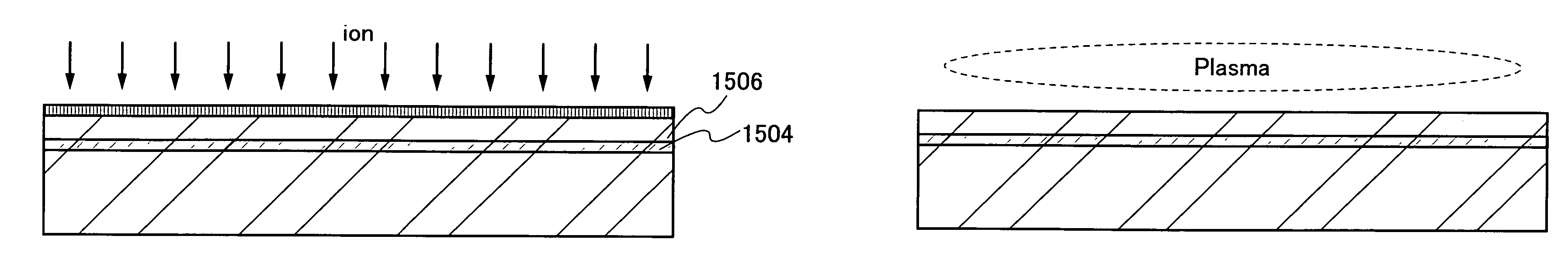
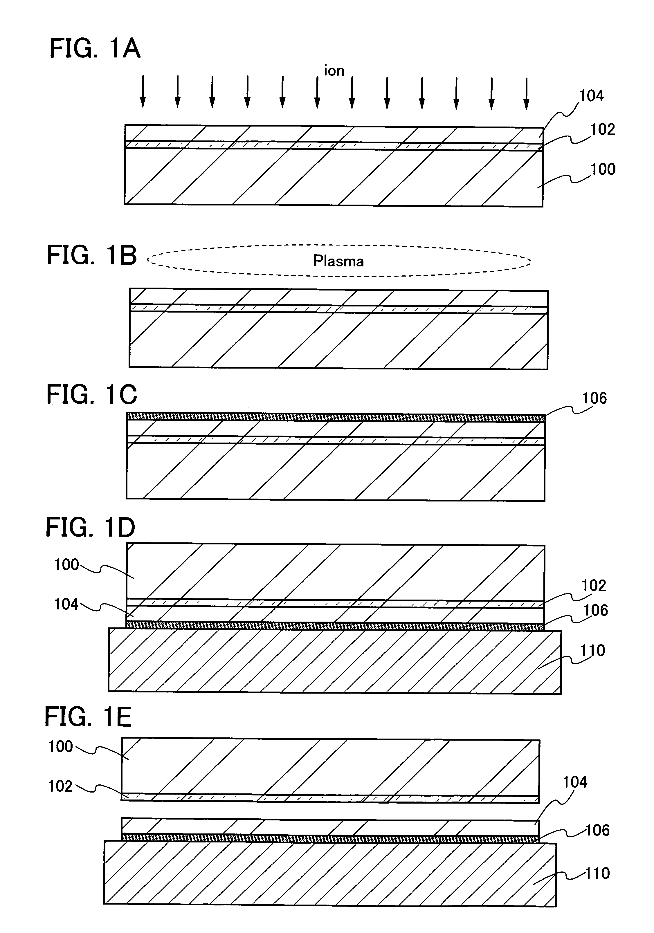
[0040]In this embodiment mode, an example of a method for manufacturing a semiconductor device of the present invention is described with reference to FIGS. 1A to 3C.

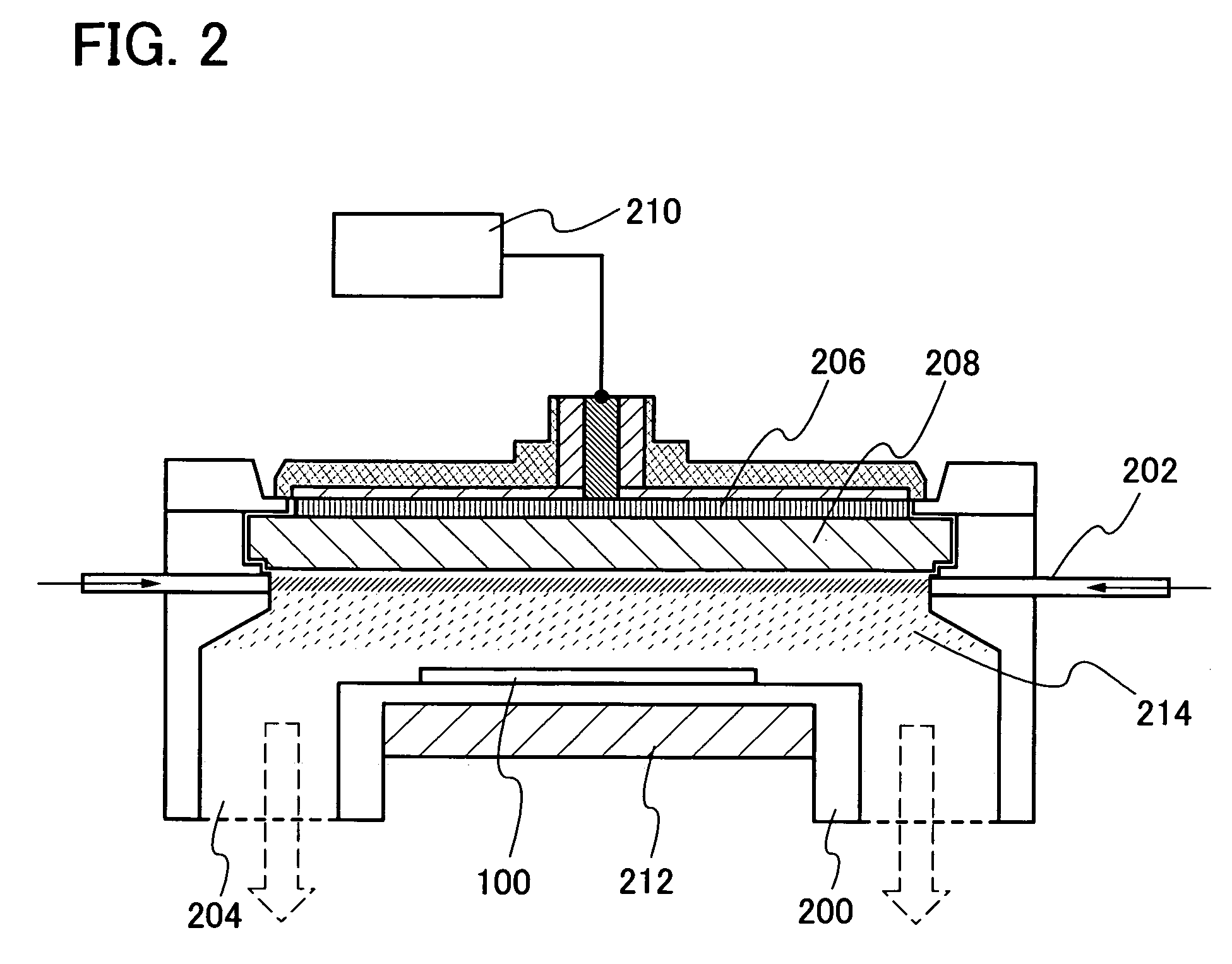
[0041]First, a single crystal semiconductor substrate 100 is prepared. Then, a surface of the single crystal semiconductor substrate 100 is irradiated with ions to introduce the ions in a given depth from a top surface so that a damaged region 102 (also referred to as an ion implanted layer or an ion doped layer) and a single crystal semiconductor layer 104 are formed (see FIG. 1A). As a formation method of the damaged region 102, a method which is used when an impurity element is added to a semiconductor layer (an ion doping method), a method in which an ionized gas is mass-separated to irradiate a semiconductor layer selectively (an ion implantation method), or the like can be given. The irradiation with the ions may be conducted in consideration of the thickness of the single crystal semiconductor layer 104 which is ...

embodiment mode 2

[0076]In this embodiment mode, another example of a method for manufacturing a semiconductor device according to the present invention is described with reference to FIGS. 4A to 4C and FIGS. 5A to 5C. In this embodiment mode, a method for manufacturing a semiconductor device in which the defect shown in Embodiment Mode 1 can be repaired and damage of a single crystal semiconductor layer due to ion irradiation can be reduced is described.

[0077]First, a protective layer 450 is formed over a single crystal semiconductor substrate 400 (see FIG. 4A). Any substrate can be used as the single crystal semiconductor substrate 400 as long as it is formed of a single crystal semiconductor material. As an example, a single crystal silicon substrate can be used. Besides, a substrate formed of a single crystal germanium, a compound semiconductor such as gallium arsenide, and indium phosphide, or the like can be used.

[0078]The protective layer 450 can be formed of one or a plurality of materials se...

embodiment mode 3

[0096]In this embodiment mode, an example of a method for manufacturing a semiconductor device of the present invention is described with reference to FIGS. 6A to 6D to FIGS. 9A and 9B. In this embodiment mode, a liquid crystal display device is described as an example of the semiconductor device; however, the semiconductor device of the invention is not limited to this.

[0097]First, a single crystal semiconductor layer is formed over a substrate having an insulating surface using any of the methods shown in Embodiment Mode 1 or Embodiment Mode 2 (see FIG. 6A). Here, a structure in which a barrier layer 602, a bonding layer 604, and a single crystal semiconductor layer 606 are provided in order over a substrate 600 having an insulating surface is described; however, the invention is not limited to this. Then, the single crystal semiconductor layer 606 and the bonding layer 604 are patterned into a desired shape, thereby forming island-shaped single crystal semiconductor layers.

[0098]...


PUM


Abstract

A single crystal semiconductor layer is formed over a substrate having an insulating surface by the following steps: forming an ion doped layer at a given depth from a surface of a single crystal semiconductor substrate; performing plasma treatment to the surface of the single crystal semiconductor substrate; forming an insulating layer on the single crystal semiconductor substrate to which the plasma treatment is performed; bonding the single crystal semiconductor substrate to the substrate having the insulating surface with an insulating layer interposed therebetween; and separating the single crystal semiconductor substrate using the ion doped layer as a separation surface. As a result, a semiconductor substrate in which a defect in an interface between the single crystal semiconductor layer and the insulating layer is reduced can be provided.

Description

BACKGROUND OF THE INVENTION[0001]1. Field of the Invention[0002]The present invention relates to a semiconductor substrate, and a method for manufacturing a semiconductor substrate, a semiconductor device, and an electronic device.[0003]2. Description of the Related Art[0004]In recent years, an integrated circuit that uses an SOI (silicon on insulator) substrate replacing a silicon wafer formed by cutting an ingot of a single crystal semiconductor into thin slice, has been developed. An SOI substrate has a structure in which a thin single crystal silicon layer is provided on an insulating surface. By using this structure, a parasitic capacitance between a drain of a transistor and a substrate can be reduced and performance of a semiconductor integrated circuit can be improved.[0005]There are various methods for manufacturing an SOI substrate; however, a Smart Cut (registered trademark) method is known for achieving both high quality and a high productivity (throughput) of a single c...

Claims


Application Information

Patent Timeline
Patent Type & Authority Patents(United States)
IPC IPC(8): H01L21/30
CPCH01L21/76254
Inventor KAKEHATA, TETSUYAKURIKI, KAZUTAKA
Owner SEMICON ENERGY LAB CO LTD
Why Eureka
Try Eureka